Epson Research and Development
Page 11
Vancouver Design Center
Interfacing to the NEC VR4102™ Microprocessor
S1D13704
Issue Date: 01/02/12
X26A-G-008-05
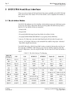
Two other configuration options (CNF[4:3]) are also made at time of hardware reset:
• endian mode setting (big endian or little endian).
• polarity of the LCDPWR signal.
The capability to select the endian mode independent of the host bus interface offers more
flexibility in configuring the S1D13704 with other CPUs.
For details on configuration, refer to the S1D13704 Hardware Functional Specification,
document number X26A-A-001-xx.
3.2 Generic #2 Interface Mode
Generic #2 interface mode is a general and non-processor-specific interface mode on the
S1D13704. The Generic # 2 interface mode was chosen for this interface due to the
simplicity of its timing and compatibility with the VR4102 control signals.
The interface requires the following signals:
• BUSCLK is a clock input which synchronizes transfers between the host CPU and the
S1D13704. It is separate from the input clock (CLKI) and is typically driven by the host
CPU system clock.
• The address inputs AB0 through AB15, and the data bus DB0 through DB15, connect
directly to the CPU address and data bus, respectively. On 32-bit big endian architec-
tures such as the Power PC, the data bus would connect to the high-order data lines; on
little endian hosts, or 16-bit big endian hosts, they would connect to the low-order data
lines. The hardware engineer must ensure that CNF3 selects the proper endian mode
upon reset.
• Chip Select (CS#) is driven by decoding the high-order address lines to select the proper
IO or memory address space.
• WE1# is the high byte enable for both read and write cycles and WE0# is the enable
signal for a write access. These must be generated by external decode hardware based
upon the control outputs from the host CPU.
• RD# is the read enable for the S1D13704, to be driven low when the host CPU is
reading data from the S1D13704. RD# must be generated by external decode hardware
based upon the control outputs from the host CPU.
• WAIT# is a signal which is output from the S1D13704 to the host CPU that indicates
when data is ready (read cycle) or accepted (write cycle) on the host bus. Since host
CPU accesses to the S1D13704 may occur asynchronously to the display update, it is
possible that contention may occur in accessing the 13704 internal registers and/or
*

