Page 26
Epson Research and Development
Vancouver Design Center
S1D13704
Hardware Functional Specification
X26A-A-001-04
Issue Date: 01/02/08
7 A.C. Characteristics
Conditions: IO V
DD
= 3.3V ± 10% or IO V
DD
= 5V ± 10%
T
A
= -40
°
C to 85
°
C
T
rise
and
T
fall
for all inputs must be < 5 nsec (10% ~ 90%)
C
L
= 60pF (Bus/MPU Interface)
C
L
= 60pF (LCD Panel Interface)
7.1 Bus Interface Timing
7.1.1 SH-4 Interface Timing
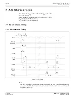
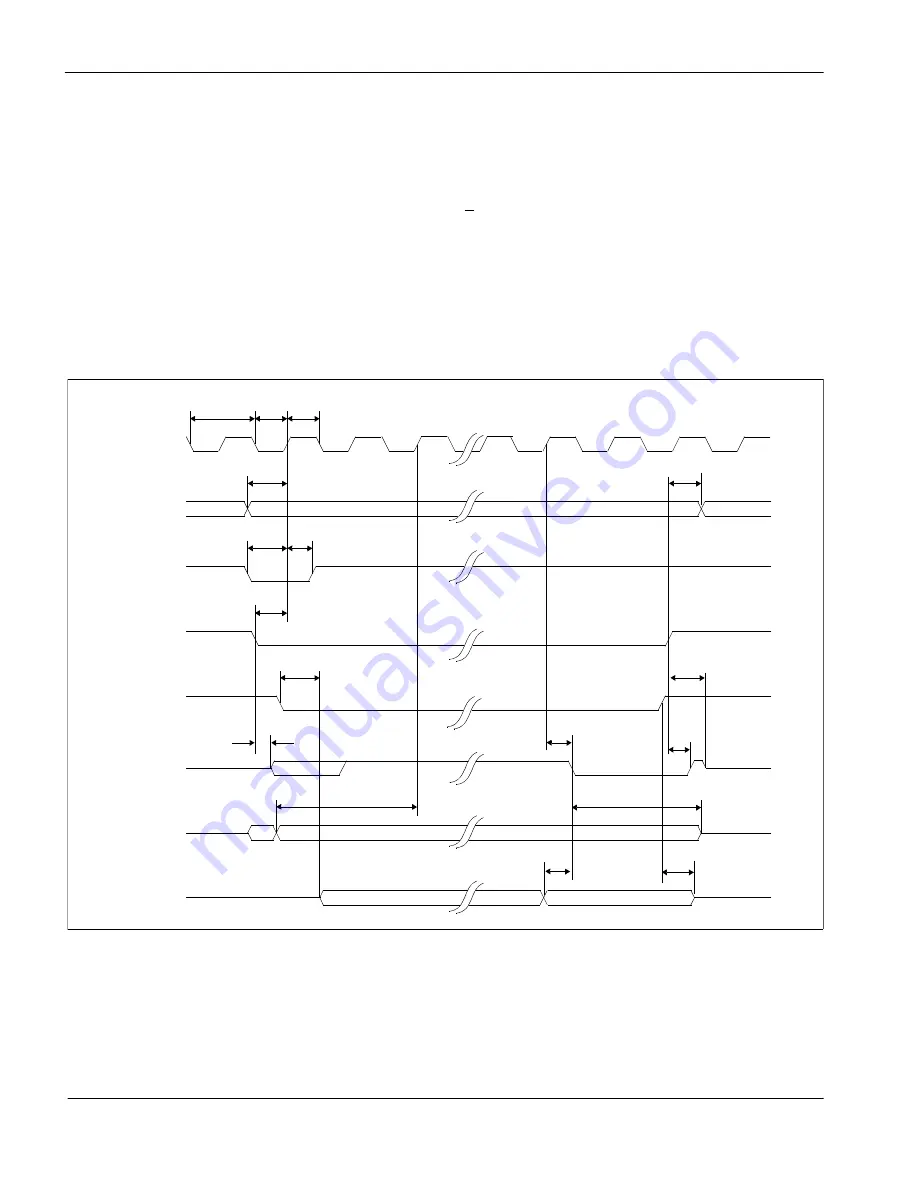
Figure 7-1: SH-4 Timing
Note
The SH-4 Wait State Control Register for the area in which the S1D13704 resides must be set to
a non-zero value. The SH-4 read-to-write cycle transition must be set to a non-zero value (with
reference to BUSCLK).
T
CKIO
t2
t3
t4
t10
t11
t16
t5
t6
t7
t8
t9
t12
t17
t15
CKIO
A[16:0]
CSn#
RD/WR#
RD#
D[15:0]
BS#
RDY#
WEn#
D[15:0]
VALID
(write)
(read)
t13
t14
*

