Epson Research and Development
Page 51
Vancouver Design Center
Hardware Functional Specification
S1D13704
Issue Date: 01/02/08
X26A-A-001-04
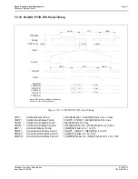
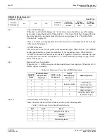
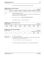
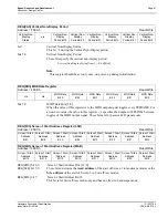
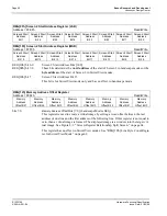
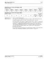
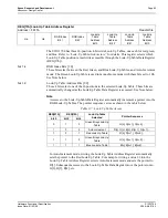
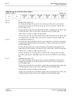
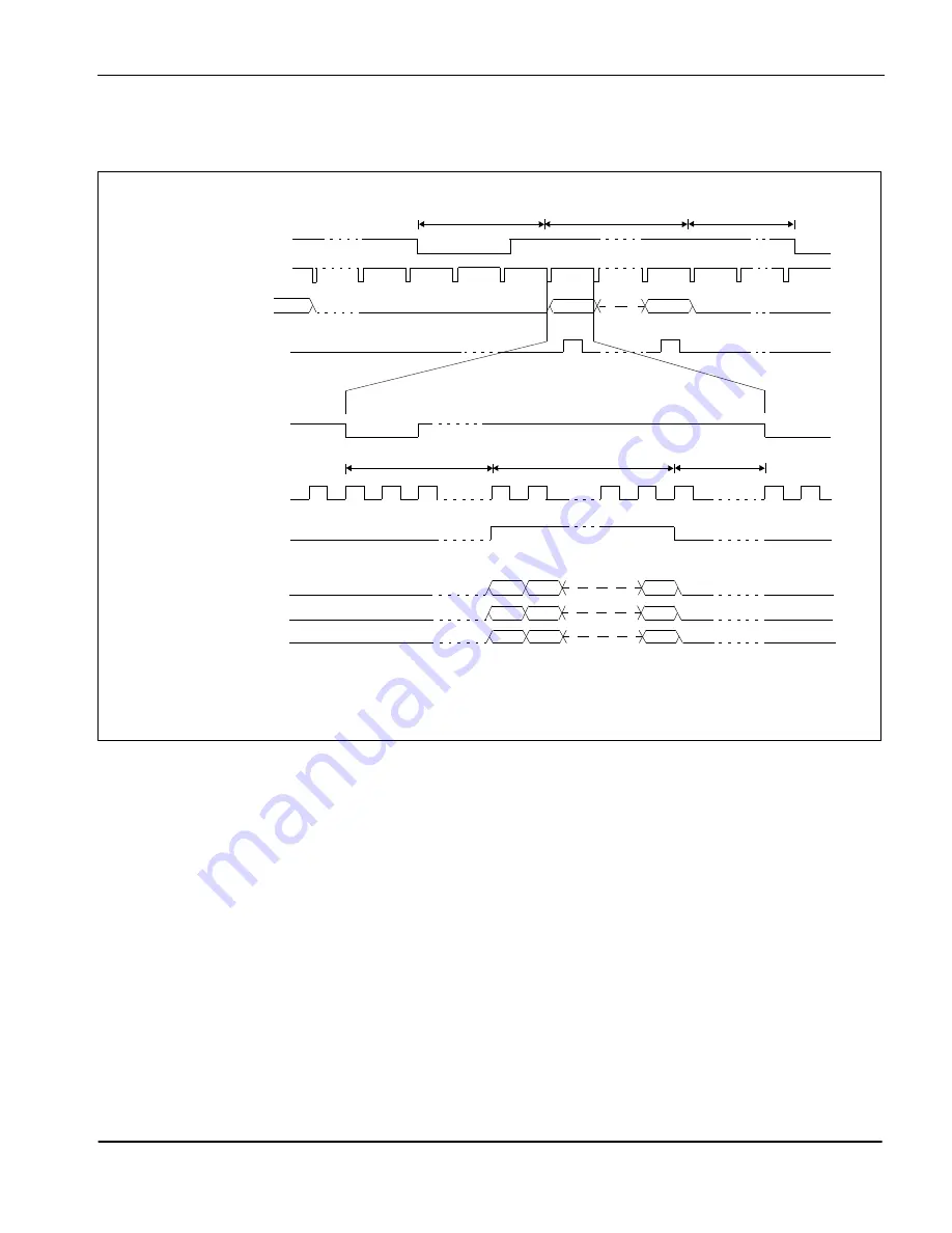
7.3.10 9/12-Bit TFT/D-TFD Panel Timing
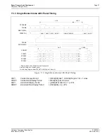
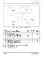
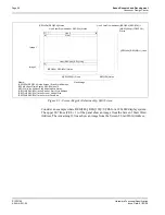
Figure 7-24: 12-Bit TFT/D-TFD Panel Timing
VDP =
Vertical Display Period
= (REG[06h] bits 1-0, REG[05h] bits 7-0) + 1 Lines
VNDP =
Vertical Non-Display Period
= VNDP1 + VNDP2 = (REG[0Ah] bits 5-0) Lines
VNDP1 =
Vertical Non-Display Period 1
= REG[09h] bits 5-0 Lines
VNDP2 =
Vertical Non-Display Period 2
= (REG[0Ah] bits 5-0) - (REG[09Ah] bits 5-0) Lines
HDP =
Horizontal Display Period
= ((REG[04h] bits 6-0) + 1) x 8Ts
HNDP =
Horizontal Non-Display Period
= HNDP1 + HNDP2 = (REG[08h] + 4) x 8Ts
HNDP1=
Horizontal Non-Display Period 1
= ((REG[07h] bits4-0) x 8) +16Ts
HNDP2=
Horizontal Non-Display Period 2
= (((REG[08h] bits4-0) - (REG[07h] bits 4-0)) x 8) +16Ts
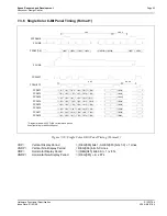
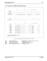
FPFRAME
FPLINE
LINE1
LINE480
1-1
1-1
1-1
1-2
1-2
1-2
1-640
1-640
1-640
FPLINE
FPSHIFT
DRDY
FPDAT[11:0]
VDP
DRDY
Note: DRDY is used to indicate the first pixel
Example Timing for 640x480 panel
VNDP
2
HDP
HNDP
2
HNDP
1
LINE480
VNDP
1
FPDAT[9]
FPDAT[10]
FPDAT[11]
FPDAT[8:6]
FPDAT[4:3]
FPDAT[2:0]
*

