Epson Research and Development
Page 67
Vancouver Design Center
Hardware Functional Specification
S1D13704
Issue Date: 01/02/08
X26A-A-001-04
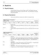
bits 3-0
Look-Up Table Data Bits [3:0]
This register is used to read/write the RGB Look-Up Tables. This register is an aperture
into the three 16-position Look-Up Tables. The Look-Up Table Address Register
(REG[16h]) selects which Look-Up Table position is accessible. See REG[16h] Look-Up
Table Bank Select Register on page 66.
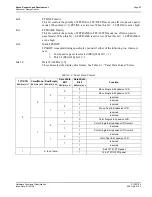
bits 4-0
GPIO[4:0] Pin IO Configuration
These bits determine the direction of the GPIO[4:0] pins.
When GPIOn Pin IO Configuration bit = 0, the corresponding GPIOn pin is configured as
an input. The input can be read at the GPIOn Status/Control Register bit. See REG[19h]
below.
When GPIOn Pin IO Configuration bit = 1, the corresponding GPIOn pin is configured as
an output. The output can be controlled by writing the GPIOn Status/Control Register bit.
Note
These bits have no effect when the GPIOn pin is configured for a specific function (i.e.
as FPDAT[11:8] for TFT/D-TFD operation). All unused GPIO pins must be tied to
IO V
DD
.
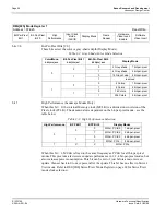
bits 4-0
GPIO[4:0] Status
When the GPIOn pin is configured as an input, the corresponding GPIO Status bit is used
to read the pin input. See REG[18h] above.
When the GPIOn pin is configured as an output, the corresponding GPIO Status bit is used
to control the pin output.
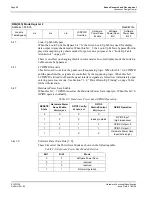
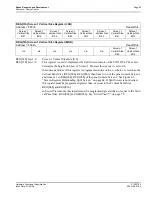
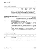
REG[17h] Look-Up Table Data Register
Address = FFF7h
Read/Write
n/a
n/a
n/a
n/a
Look-Up
Table Data
Bit 3
Look-Up
Table Data
Bit 2
Look-Up
Table Data
Bit 1
Look-Up
Table Data
Bit 0
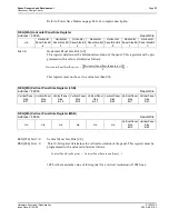
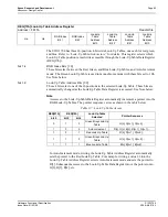
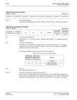
REG[18h] GPIO Configuration Control Register
Address = FFF8h
Read/Write
n/a
n/a
n/a
GPIO4 Pin IO
Configuration
GPIO3 Pin IO
Configuration
GPIO2 Pin IO
Configuration
GPIO1 Pin IO
Configuration
GPIO0 Pin IO
Configuration
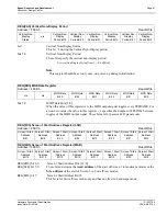
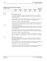
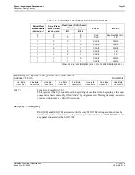
REG[19h] GPIO Status/Control Register
Address = FFF9h
Read/Write
n/a
n/a
n/a
GPIO4 Pin IO
Status
GPIO3 Pin IO
Status
GPIO2 Pin IO
Status
GPIO1 Pin IO
Status
GPIO0 Pin IO
Status
*


