Page 26
Epson Research and Development
Vancouver Design Center
S1D13704
Programming Notes and Examples
X26A-G-002-03
Issue Date: 01/02/12
5.1.1 Registers
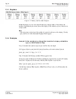
Figure 5-2: Memory Address Offset Register
REG[12h] forms an 8-bit value called the Memory Address Offset. This offset is the
number of additional bytes on each line of the display. If the offset is set to zero there is no
virtual width.
Note
This value does not represent the number of words to be shown on the display. The dis-
play width is set in the Horizontal Display Width register.
5.1.2 Examples
Example 1: In this example we go through the calculations to display a 640x480 im-
age on a 320x240 panel at 2 bpp.
Step 1: Calculate the number of pixels per word for this color depth.
At 2 bpp each byte is comprised of 4 pixels, therefore each word contains 8 pixels.
pixels_per_word = 16 / bpp = 16 / 2 = 8
Step 2: Calculate the Memory Address Offset register value
We require a total of 640 pixels. The horizontal display register will account for 320 pixels,
this leaves 320 pixels for the Memory Address Offset register to account for.
offset = pixels / pixels_per_word = 320 / 8 = 40 = 28h
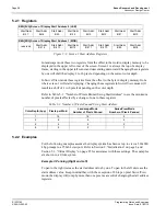
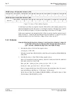
The Memory Address Offset register, REG[12h], will have to be set to 28h to satisfy the
above condition.
REG[12h] Memory Address Offset Register
Memory
Address
Offset
Bit 7
Memory
Address
Offset
Bit 6
Memory
Address
Offset
Bit 5
Memory
Address
Offset
Bit 4
Memory
Address
Offset
Bit 3
Memory
Address
Offset
Bit 2
Memory
Address
Offset
Bit 1
Memory
Address
Offset
Bit 0
*

