Page 86
Epson Research and Development
Vancouver Design Center
S1D13704
Hardware Functional Specification
X26A-A-001-04
Issue Date: 01/02/08
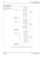
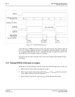
Figure 13-1: Panel On/Off Sequence
After chip reset, LCDPWR is inactive and the rest of the panel interface output signals are
held ‘low’. Software initializes the chip (i.e. programs the registers) and then - as a last step
set - programs REG[03h] bits [1:0] to 11. This starts the power-up sequence as shown. The
power-up/power-down sequence delay is 127 frames.
The power-up/power-down sequence also occurs when exiting/entering Software Power
Save Mode.
13.5 Turning Off BCLK Between Accesses
BCLK may be turned off (held low) between accesses if the following rules are observed:
1. BCLK must be turned off/on in a glitch free manner
2. BCLK must continue for a period equal to [8T
BCLK
+ 12T
MCLK
] after the end of the
access (RDY# asserted or WAIT# deasserted).
3. BCLK must be present for at least one T
BCLK
before the start of an access.
RESET#
LCDPWR
Panel Interface
Output Signals
(except LCDPWR)
0 frame
127 frames
0 frame
Power Save Mode
power-down
power-up
power-up
Software Power Save
00
11
00
11
(CNF4 = Low)
LCDPWR
(CNF4 = Hi)
Hardware Power Save
REG[03h] bits [1:0]
or
*

