background image

MF302-13

Technical Manual

S1F70000 Series 

T

echnical Manual

IEEE1394 Controller

S1R77801F00A

Technical Manual

S1F70000 Series

EPSON Electronic Devices Website

ELECTRONIC DEVICES MARKETING DIVISION

First issue November,1990 U 


Revised July,2001 in Japan H


B

4.5mm

Technical Manual

POWER SUPPLY IC

S1F70000 Series

http://www.epson.co.jp/device/

This manual was made with recycle paper,
and printed using soy-based inks.

Summary of Contents for S1F76610C0B0

Page 1: ...nual S1F70000 Series EPSON Electronic Devices Website ELECTRONIC DEVICES MARKETING DIVISION First issue November 1990 U Revised July 2001 in Japan H B 4 5mm Technical Manual POWER SUPPLY IC S1F70000 Series http www epson co jp device This manual was made with recycle paper and printed using soy based inks ...

Page 2: ...ty that anything made in accordance with this material will be free from any patent or copyright infringement of a third party This material or portions thereof may contain technology or the subject relating to strategic products under the control of the Foreign Exchange and Foreign Trade Low of Japan and may require an export licenes from the Ministry of International Trade and Industry or other ...

Page 3: ...ous number Previous number New number SCI7660M0B S1F76600M0B0 SCI7660C0B S1F76600C0B0 SCI7662M0A S1F76620M0A0 SCI7662D0A S1F76620D0A0 SCI7661M0B S1F76610M0B0 SCI7661MBB S1F76610M2B0 SCI7661C0B S1F76610C0B0 SCI7654M0A S1F76540M0A0 SCI7654C0A S1F76540C0A0 SCI7664M0A S1F76640M0A0 SCI7664D0A S1F76640D0A0 SCI7810Y B S1F78100Y2 0 SCI7910Y A S1F79100Y1 0 SCI7631MLA S1F76310M1L0 SCI7631MBA S1F76310M1B0 SC...

Page 4: ...S1F70000 Series Technical Manual ...

Page 5: ...CATIONS 1 8 S1F76620 Series DESCRIPTION 1 10 FEATURES 1 10 BLOCK DIAGRAM 1 10 PIN DESCRIPTIONS 1 11 FUNCTIONAL DESCRIPTIONS 1 13 ELECTRICAL CHARACTERISTICS 1 14 EXAMPLE OF REFERENCE EXTERNAL CONNECTION 1 21 MEASUREMENT CIRCUIT 1 24 MECHANICAL DATA 1 25 2 DC DC Converter Voltage Regulator S1F76610 Series DESCRIPTION 2 1 FEATURES 2 1 APPLICATIONS 2 1 BLOCK DIAGRAM 2 1 PIN ASSIGNMENTS 2 2 PIN DESCRIP...

Page 6: ...SSIGNMENTS 2 40 PIN DESCRIPTIONS 2 41 CHIP EXTERNAL SHAPE AND PAD CENTER COORDINATES 2 42 FUNCTIONAL DESCRIPTIONS 2 43 ELECTRICAL CHARACTERISTICS 2 46 CHARACTERISTICS GRAPH 2 51 MECHANICAL DATA 2 56 APPLICATION EXAMPLE 2 57 3 Voltage Regulator S1F78100Y Series DESCRIPTION 3 1 FEATURES 3 1 BLOCK DIAGRAM 3 1 PIN DESCRIPTIONS 3 2 PIN ASSIGNMENTS 3 2 FUNCTIONAL DESCRIPTIONS 3 3 LINEUP 3 4 ABSOLUTE MAX...

Page 7: ...PTIONS 3 35 TYPICAL APPLICATIONS 3 36 4 DC DC Switching Regulators S1F76300 Series S1F76310 S1F76380 Series DESCRIPTION 4 1 FEATURES 4 1 APPLICATIONS 4 1 LINEUP 4 1 BLOCK DIAGRAMS 4 2 PIN ASSIGNMENTS 4 3 PIN DESCRIPTIONS 4 3 SPECIFICATIONS 4 4 PACKAGE MARKINGS 4 13 FUNCTIONAL DESCRIPTIONS 4 13 TYPICAL APPLICATIONS 4 15 S1F76330 Series DESCRIPTION 4 22 FEATURES 4 22 APPLICATIONS 4 22 LINEUP 4 22 BL...

Page 8: ...TIONAL DESCRIPTIONS 4 36 ABSOLUTE MAXIMUM RATINGS 4 37 ELECTRICAL CHARACTERISTICS 4 38 EXAMPLE OF EXTERNAL CONNECTION OF REFERENCE CIRCUIT 4 39 MECHANICAL DATA 4 40 S1F71200 Series DESCRIPTION 4 41 FEATURES 4 41 BLOCK DIAGRAM 4 42 PIN ASSIGNMENTS 4 43 PIN DESCRIPTIONS 4 44 FUNCTIONAL DESCRIPTIONS 4 45 ABSOLUTE MAXIMUM RATINGS 4 47 ELECTRICAL CHARACTERISTICS 4 48 EXAMPLE OF EXTERNAL CONNECTION OF R...

Page 9: ...Y Series 5 21 PRECAUTIONS 5 22 6 Appendix ABSOLUTE MAXIMUM RATINGS 6 1 RECOMMENDER OPERATING CONDITIONS 6 1 ELECTRICAL CHARACTERISTICS 6 1 POWER DISSIPATION CONDITIONS 6 1 PARAMETER SUMMARY 6 2 MECHANICAL DATA 6 4 EMBOSS CARRIER TAPING STANDARD SOT89 3pin TAPING INFORMATION 6 6 REEL SPECIFICATIONS 6 7 DEVICE POSITIONING 6 7 EMBOSS CARRIER TAPING STANDARD SOP3 8pin TAPING INFORMATION 6 8 REEL SPECI...

Page 10: ...Contents vi EPSON S1F70000 Series Technical Manual EMBOSS CARRIER TAPING STANDARD SOP2 24pin TAPING INFORMATION 6 14 REEL SPECIFICATIONS 6 16 DEVICE POSITIONING 6 16 ...

Page 11: ...ance and packaging We suggest that you use the selector guide beginning on the following page to choose the IC or IC series that most closely matches your application Then you can use the detailed product descriptions in subsequent sections to confirm device specifications and charac teristics Please contact your local SEIKO EPSON sales representative for further information or assistance on these...

Page 12: ...oltage stability Typ 0 1 V Voltage regulator Product Features Package Supply voltage conversion IC S1F76600M0B0 It effectively converts input voltage VDD into VDD or 2VDD SOP4 8pin S1F76600C0B0 Output current Max 30mA at 5V DIP 8pin Power conversion efficiency Typ 95 Supply voltage conversion IC It effectively converts input voltage VDD into VDD or 2VDD S1F76620M0A0 Output current Max 30mA at 5V S...

Page 13: ...rent Typ 4 0 µA SOT89 3pin Input voltage stability Typ 0 1 V 3 00V negative output voltage regulator S1F79100Y1D0 Low operating current Typ 4 0 µA SOT89 3pin Input voltage stability Typ 0 1 V 1 80V negative output voltage regulator S1F79100Y1G0 Low operating current Typ 4 0 µA SOT89 3pin Input voltage stability Typ 0 1 V 1 50V negative output voltage regulator S1F79100Y1H0 Low operating current Ty...

Page 14: ... 5mV C Step up switching regulator from 1 5V to 2 4V Low operating voltage Min 0 9V Low operating current Typ 7µA S1F76380M1L0 Built in CR oscillator circuit SOP3 8pin High precision voltage detection Output voltage response compensation Temperature characteristics of output voltage for LCD panel 4 0mV C Step up switching regulator from 1 5V to 3 0V Low operating voltage Min 0 9V S1F76330M1B0 Low ...

Page 15: ...t format COMS SOP89 3pin Low operating power Typ 2 0 µA VDD 3 0V Voltage detection Typ 2 55V S1F77210Y1E0 Output format COMS SOP89 3pin Low operating power Typ 2 0 µA VDD 3 0V Voltage detection Typ 2 35V S1F77210Y1S0 Output format COMS SOP89 3pin Low operating power Typ 2 0 µA VDD 3 0V Voltage detection Typ 2 25V S1F77210Y1P0 Output format COMS SOP89 3pin Low operating power Typ 2 0 µA VDD 3 0V Vo...

Page 16: ...Output format N ch open drain SOP89 3pin Low operating power Typ 1 5 µA VDD 1 5V Voltage detection Typ 1 05V S1F77200Y1A0 Output format N ch open drain SOP89 3pin Low operating power Typ 1 5 µA VDD 1 5V Voltage detection Typ 0 95V S1F77200Y1V0 Output format N ch open drain SOP89 3pin Low operating power Typ 1 5 µA VDD 1 5V Voltage detection Typ 1 25V S1F77220Y2D0 Output format P ch open drain SOP8...

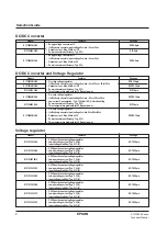
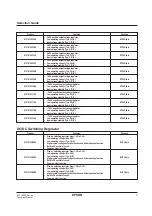
Page 17: ...1 DC DC Converter ...

Page 18: ...eries Low operating voltage On chip CR oscillator 8 pin plastic DIP and 8 pin plastic SOP APPLICATIONS Fixed voltage power supplies for battery operated equipment Power supplies for pagers memory cards calculators and similar hand held equipment Fixed voltage power supplies for medical equipment Fixed voltage power supplies for communications equipment Uninterruptable power supplies BLOCK DIAGRAM ...

Page 19: ...vices Recommended Operating Conditions VDD 0V Ta 40 to 85 C unless otherwise noted Parameter Symbol Condition Rating Unit Min Typ Max ROSC 1MΩ C1 C2 1 20 C2 10µF 1 5 Oscillator startup voltage VSTA Ta 20 to 85 C V See note 1 ROSC 1MΩ 2 2 Oscillator shutdown voltage VSTP ROSC 1MΩ 1 5 V Load resistance RL RL min Ω See note 2 Output current IO 30 0 mA Clock frequency fOSC 10 0 30 0 kHz CR oscillator ...

Page 20: ...OSC 1MΩ 20 30 µA VI 5V Quiescent current IQ RL VI 8V 2 0 µA Clock frequency fOSC ROSC 1MΩ VI 5V 16 20 24 kHz Output impedance RO IO 10mA VI 5V 75 100 Ω Multiplication efficiency Peff IO 5mA VI 5V 90 95 OSC1 Input leakage current ILKI VI 8V 2 0 µA 3 RL min is a function of VI Electrical Characteristics Battery C L D1 C2 22µF C1 10µF R L 1MΩ 8 7 6 5 1 2 3 4 1 0 5 4 3 2 1 0 1 5 2 0 Input voltage V Mi...

Page 21: ...7 16 15 14 13 12 11 10 9 8 40 20 0 20 40 Ta C f OSC kHz 60 80 100 VI 5 0V VI 3 0V VI 2 0V 1 Clock frequency vs External resistance 2 Clock frequency vs Ambient temperature 50 45 40 35 30 25 20 15 10 5 0 7 6 5 4 3 2 1 0 l OPR µA VI V Ta 25 C fOSC 40kHz fOSC 20kHz fOSC 10kHz 0 5 10 15 0 10 20 30 40 50 V O V IO mA Ta 25 C VI 5 0V 3 Multiplier current vs Input voltage 4 Output voltage vs Output curren...

Page 22: ...V 0 1 2 3 4 5 6 0 2 3 4 5 6 7 8 9 10 1 V O V IO mA Ta 25 C VI 2 0V 5 Output voltage vs Output current 6 Output voltage vs Output current 300 200 100 0 7 6 5 4 3 2 1 0 R O Ω VI V Ta 25 C IO 7mA 300 200 100 0 7 6 5 4 3 2 1 0 R O Ω VI V Ta 25 C IO 10mA 7 Output impedance vs Input voltage 8 Output impedance vs Input voltage ...

Page 23: ...V 9 Multiplication efficiency vs 10 Multiplication efficiency vs Clock frequency Clock frequency 100 90 80 70 60 50 40 30 20 10 0 100 90 80 70 60 50 40 30 20 10 0 0 10 20 30 40 50 Peff I I mA IO mA Ta 25 C VI 5 0V II Peff 100 90 80 70 60 50 40 30 20 10 0 100 90 80 70 60 50 40 30 20 10 0 0 5 10 15 20 25 30 Peff I I mA IO mA Ta 25 C VI 3 0V II Peff 11 Multiplication efficiency input current 12 Multi...

Page 24: ...40 36 32 28 24 20 16 12 8 4 0 0 1 2 3 4 5 6 7 8 9 10 Peff I I mA IO mA Ta 25 C VI 2 0V II Peff 13 Multiplication efficiency input current vs Output current Voltage Multiplier The voltage multiplier uses the clock signal from the oscillator to double the input voltage This requires two external capacitors a charge pump capacitor C1 be tween CAP1 and CAP1 and a smoothing capacitor C2 between VI and ...

Page 25: ...5 V VO 10 V 1MΩ 8 7 6 5 1 2 3 4 C1 10µF 1MΩ 8 7 6 5 1 2 3 4 Serial Connection Connecting two or more chips in series obtains a higher output voltage than can be obtained using a parallel connection however this also raises the output imped ance Potential levels 5 V C1 10µF C2 10µF VDD 0 V VI 5 V VO 15 V VO 10 V VI VDD VI 5 1MΩ 8 7 6 5 1 2 3 4 C1 10µF C2 10µF 1MΩ 8 7 6 5 1 2 3 4 VDD 0 V VI 5 V VO 1...

Page 26: ...ltage positive 5 V C2 10µF VDD 0 V VO 3 8 V VI 5 V 1MΩ C1 10µF 8 7 6 5 1 2 3 4 Simultaneous Voltage Conversion Combining a multiplier circuit with a positive voltage conversion circuit generates both 10 and 3 8 V outputs from a single input Potential levels 5 V C2 10µF VDD 0 V VO2 3 8 V VO1 10 V VI 5 V 1MΩ C3 C4 10µF 10µF 8 7 6 5 1 2 3 4 C1 10µF VO2 3 8 V VO1 10 V VDD 0 V VI 5 V ...

Page 27: ...dy devices etc due to its small power consumption FEATURES 1 High efficiency and low power consumption CMOS DC DC converter 2 Easy voltage conversion from input voltage VDD 5V to positive potential side or negative potential side Input VDD 5V to output VDD 5V 2VDD 10V 3 Output current Max 30mA VDD 5V 4 Power conversion efficiency Typ 95 5 Possibility of series connection In 2 piece use VDD 5V VO 1...

Page 28: ...nus side System GND Oscillation resistor connection pin Works as the clock input pin when the external clock operates Oscillation resistor connection pin Opens when the external clock operates Power pin Plus side System VCC Pump up capacitor minus side connection pin for 2 times step up Pump up capacitor plus side connection pin for 2 times step up Output pin at the time of 2 times step up Pin nam...

Page 29: ... GND VSS OSC1 OSC2 VDD CAP1 CAP1 NC VO NC NC NC Pad center coordinates X µm 984 984 Pad center coordinates Y µm 1096 788 580 390 96 218 510 802 1094 1134 892 514 182 372 750 942 1134 Description Input pin for power off control Power input pin Minus side Oscillation resistor connection pin Oscillation resistor connection pin Power input pin Plus side Pump up capacitor minus side connection pin for ...

Page 30: ...ormula as far as the straight portion 500kΩ ROSC 2MΩ is concerned ROSC A 1 fOSC A Constant When GND is 0V and VDD is 5V A is approximately 2 0 1010 I F So the ROSC value can be obtained from this formula Recommended oscillation frequency 10kHz to 30kHz ROSC 2MΩ to 680kΩ When the external clock operates make the pin OSC2 open as shown below and input the 50 duty of the ex ternal clock from the pin ...

Page 31: ...itions of the above absolute maximum ratings may deteriorate the reliability remarkably Note 2 All voltage values are based on GND being 0V Max 10 0 VDD 0 5 20 VDD 0 5 VO 0 5 300 150 85 150 Min 0 5 0 5 0 5 0 5 40 65 Parameter Input supply voltage Input pin voltage Output voltage Output supply voltage Output pin voltage Allowable loss Operating temperature Storage temperature Symbol VIN VI VO VCAP ...

Page 32: ...ommended to be not more than 0 6V VO CAP1 CAP1 VDD 1 2 3 4 8 7 6 5 Recommended Circuit Note 3 RLmin varies with input voltage See Characteristics Graph 15 Max 1 5 30 30 2000 Parameter Step up start operation Step up stop voltage Output load resistance Output load current Oscillation frequency External resistor for oscillation Step up capacitor Symbol VSTA1 VSTA2 VSTP RL IO fOSC ROSC C1 C2 Rating M...

Page 33: ...uit current consumption Static current Oscillation frequency Output impedance Step up power conver sion efficiency Input leak current Symbol VDD VO IOPR IQ fOSC RO Peff ILKI Rating Min 1 8 16 90 Typ 35 20 85 95 Max 8 0 16 0 50 1 0 24 130 1 0 Unit V V µA µA kHz Ω µA Remarks ROSC 1MΩ ROSC 1MΩ IO 10mA IO 5mA OSC1 pin Note 1 All voltage values are based on GND being 0V ...

Page 34: ...ent consumption vs Input current 4 Output voltage VO vs Output current 1 40 20 0 20 40 60 80 100 30 28 26 24 22 20 18 16 14 12 10 f OSC kHz Ta C VDD 5V VDD 2V VDD 3V 10 100 1000 10000 Ta 25 C VDD 5V VDD 3V VDD 2V ROSC kΩ f OSC kHz 1000 100 10 1 0 5 10 15 20 25 30 10 9 8 7 6 5 4 3 2 1 0 V O V IO mA Ta 25 C VDD 5V C1 C2 10µF 0 1 2 3 4 5 6 100 80 60 40 20 0 I OPR1 µA VDD V Ta 25 C C1 C2 10µF fOSC 40k...

Page 35: ... Output impedance vs Input current 1 8 Output impedance vs Input voltage 2 4 3 2 1 0 6 5 4 3 2 1 0 0 1 2 3 4 5 6 7 8 9 10 0 5 10 15 20 V O V IO mA IO mA V O V Ta 25 C VDD 3V C1 C2 10µF Ta 25 C VDD 2V C1 C2 10µF 300 250 200 150 100 50 0 0 1 2 3 4 5 6 VDD V R O Ω Ta 25 C IO 10mA 300 250 200 150 100 50 0 0 1 2 3 4 5 6 VDD V R O Ω Ta 25 C IO 5mA ...

Page 36: ...0 70 60 50 40 30 20 10 0 100 90 80 70 60 50 40 30 20 10 0 0 5 10 15 20 IO mA Peff I DD mA Ta 25 C VDD 3V C1 C2 10µF 100 90 80 70 60 50 40 30 20 10 0 150 120 90 60 30 0 0 10 20 30 IO mA Peff I DD mA Ta 25 C VDD 5V C1 C2 10µF 100 90 80 70 60 50 40 30 20 10 0 100 90 80 70 60 50 50 40 30 20 10 0 1 10 100 1000 0 1 2 3 4 5 6 7 8 9 10 IO 5mA IO 2mA IO 20mA IO 10mA focs kHz IO mA Peff Peff I DD mA Ta 25 C...

Page 37: ...cillation frequency 3 15 Step up start voltage 1 vs Load resistance 100 90 80 70 60 50 1 10 100 1000 IO 0 5mA IO 1mA IO 5mA IO 2mA focs kHz Peff Ta 25 C VDD 2V C1 C2 10µF 100 90 80 70 60 50 1 10 100 1000 focs kHz Peff IO 1mA IO 2mA IO 10mA IO 5mA Ta 25 C VDD 3V C1 C2 10µF 1 7 1 6 1 5 1 4 1 3 1 2 1 1 1 0 0 9 100 1000 10000 100000 RL Ω V STA1 V Ta 25 C C1 C2 10µF ROSC 1MΩ ...

Page 38: ... 1 2 3 4 8 7 6 5 Figure 1 2 Time Step up Operation Parallel Connection It is possible to make the output impedance RO small when several pieces of the circuit shown in Figure 1 are connected Parallel connection of n circuits reduces RO to 1 n approximately One piece of the smoothing capacitor C2 can be commonly used POFF VI _ _ GND OSC1 OSC2 VO CAP1 CAP1 VDD 1 2 3 4 8 7 _ 6 5 POFF GND OSC1 OSC2 VO...

Page 39: ... POFF VI GND OSC1 OSC2 VO CAP1 CAP1 VDD 1 2 3 4 8 7 6 5 POFF GND OSC1 OSC2 VO Vo 3 VI Vo 2 VI CAP1 CAP1 VDD 1 2 3 4 6 5 8 7 Figure 3 Series Connection VDD VO 10V VO 15V VDD 5V GND 0V GND First stage Next stage Figure 4 Power Supply Relations in Series Connection 1 Note When the input voltage in the next stage is as per the specification VDD GND 8V in a series connection the output in the first sta...

Page 40: ... 3 4 8 7 5 6 Figure 6 Negative Voltage Conversion Negative Voltage Conversion Positive Voltage Conversion When the 3 times step up operation shown in Figure 1 and the positive voltage conversion in Figure 6 are combined the circuit shown in Figure 7 can be formed and 10V and 3 8V can be obtained from the input 5V However the output impedance is higher than in case of connection of either one only ...

Page 41: ...S1F76620 Series 1 24 EPSON S1F70000 Series Technical Manual MEASUREMENT CIRCUIT POFF VI GND OSC1 C2 VO IO RL C1 ROSC IOPR OSC2 VO CAP1 CAP1 VDD 1 2 3 A A 4 8 7 6 5 V V ...

Page 42: ... D1 A A1 A2 e b C θ L L1 L2 HE D θ2 θ3 R R1 Dimension in Milimeters Min 4 8 0 25 0 05 6 4 4 8 Nom 5 1 75 0 15 1 6 1 27 0 35 0 15 0 55 6 8 5 Max 5 2 0 45 0 25 7 2 5 2 Dimension in Inches Min 0 189 0 010 0 002 0 252 0 189 Nom 0 197 0 069 0 006 0 063 0 050 0 014 0 006 0 022 0 268 0 197 Max 0 204 0 017 0 009 0 283 0 204 Reference Note This drawing is subject to change without notice for improvement ...

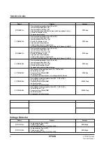
Page 43: ...2 DC DC Converter Voltage Regulator ...

Page 44: ...0 4 and 0 6 C VDD Voltage multiplier 1 Voltage multiplier 2 CR oscilator Reference voltge generator Temperature gradient selector Voltage regulator TC1 TC2 RV POFF VREG VO VI OSC2 OSC1 CAP1 CAP1 CAP2 CAP2 Multiplication stage Stabilization stage BLOCK DIAGRAM S1F76610 Series CMOS DC DC Converter Voltage Doubler Tripler Voltage Regulator External shut down control 2µA maximum output current when sh...

Page 45: ...ier Negative charge pump connection for 2 multiplier Positive charge pump connection for 3 multiplier Negative charge pump connection for 3 multiplier or 2 multiplier output Pin No 1 2 3 4 5 6 7 8 9 10 11 12 13 14 Pin name CAP1 CAP1 CAP2 CAP2 TC1 TC2 VI VO VREG RV POFF OSC2 OSC1 VDD Temperature gradient selects Negative supply system ground 3 multiplier output Voltage regulator output Voltage regu...

Page 46: ...d 2 2V is shown in the following figure Note that diode D1 should have a maximum forward voltage of 0 6V with 1 0mA forward current 2 RL min can be varied depending on the input voltage Rating Parameter Symbol Conditions Oscillator startup voltage Oscillator shutdown voltage Load resistance Output current Clock frequency CR oscillator network resistance Capacitance Stabilization voltage sensing re...

Page 47: ...oad resistance kΩ 6 5 4 3 2 1 5 VSTA2 VSTA1 Voltage tripler Voltage doubler Symbol Parameter Conditions Input voltage Output voltage Regulator voltage Stabilization circuit operating voltage Multiplier current Stabilization current Quiescent current Clock frequency VI VO VREG VO IOPR1 IOPR2 IQ fOSC RL RRV 1MΩ VO 18V RL ROSC 1MΩ RL RRV 1MΩ VO 15V TC2 TC1 VO RL ROSC 1MΩ Rating Min 6 0 18 0 18 0 18 0...

Page 48: ...ient POFF TC1 TC2 OSC1 and RV input leakage current Symbol RO Peff RSAT VRV CT ILKI VREG IO Conditions IO 10mA IO 5mA VREG VO VREG VO 18 to 8V VREG 8V RL Ta 25 C VO 15V VREG 8V Ta 25 C IO 0 to 10µA TC1 VDD TC2 VO RSAT VREG VO IO IO 0 to 10µA RV VDD Ta 25 C TC2 TC1 VO Ta 25 C TC2 VDD TC1 VO Ta 25 C See note Rating Min 90 0 2 3 1 7 1 1 0 25 0 5 0 7 Typ 150 95 0 0 2 5 0 8 0 1 5 1 3 0 9 0 1 0 4 0 6 Ma...

Page 49: ...6 15 14 13 12 11 10 9 8 40 20 0 20 40 60 80 100 Ta C f OSC kHz VI 5 0V VI 3 0V VI 2 0V 1 Clock frequency vs External resistance 2 Clock frequency vs Ambient temperature 150 100 50 0 7 6 5 4 3 2 1 0 VI V I OPR µA fOSC 40kHz fOSC 20kHz fOSC 10kHz Ta 25 C 0 5 10 15 0 10 20 30 40 IO mA V O V Ta 25 C VI 5 0V 2 multiplier 3 multiplier 3 Multiplier current vs Input voltage 4 Output voltage vs Output curr...

Page 50: ...ut current 100 90 80 70 60 50 40 30 20 10 0 100 90 80 70 60 50 40 30 20 10 0 0 10 20 30 40 50 IO mA I I mA Peff 3 multiplier II Ta 25 C VI 5 0V 2 multiplier Peff 3 multiplier Peff 2 multiplier II 0 5 10 15 20 25 30 IO mA 60 54 48 42 36 30 24 18 12 6 0 I I mA 100 90 80 70 60 50 40 30 20 10 0 Peff Ta 25 C VI 3 0V 3 multiplier II 3 multiplier Peff 2 multiplier Peff 2 multiplier II 7 Multiplication ef...

Page 51: ... 300 200 100 0 7 6 5 4 3 2 1 0 VI V R O Ω Ta 25 C IO 6mA 3 multiplier 2 multiplier 9 Multiplication efficiency input current 10 Output impedance vs Input voltage vs Output current 7 6 5 4 3 2 1 0 VI V 500 400 300 200 100 0 R O Ω 3 multiplier Ta 25 C IO 10mA 2 multiplier 100 90 80 70 60 50 1 10 100 1000 fOSC kHz Peff IO 2mA IO 5mA IO 10mA IO 20mA IO 30mA Ta 25 C VI 5 0V 11 Output impedance vs Input...

Page 52: ...850 7 900 7 950 8 000 0 0001 0 0010 0 0100 0 1000 Ta 25 C V REG V IO V 13 Multiplication efficiency vs Clock frequency 14 Output voltage vs Output current 5 850 5 900 5 950 6 000 0 0001 0 0010 0 0100 0 1000 V REG V IO V VO 9V Ta 25 C 2 850 2 900 2 950 3 000 V REG V 0 0001 0 0010 0 0100 0 1000 IO V VO 6V Ta 25 C 15 Output voltage vs Output current 16 Output voltage vs Output current ...

Page 53: ...e regu lator output in applications such as power supplies for driving LCDs Notes 1 The definition of LOW for POFF differs from that for TC1 and TC2 2 The temperature gradient affects the voltage between VDD and VREG POFF 1 VDD 1 VDD 1 VDD 1 VDD 0 VI 0 VI 0 VI 0 VI TC2 See note 1 Low VO Low VO High VDD High VDD Low VO Low VO High VDD High VDD TC1 Low VO High VDD Low VO High VDD Low VO High VDD Low...

Page 54: ...ies a reference voltage to the voltage regulator to control the output This voltage can be switched ON and OFF VDD VREG RRV 100 kΩ to 1 MΩ RV POFF Control signal Voltage Multiplier The voltage multiplier uses the clock signal from the oscillator to double or triple the input voltage This re quires three external capacitors two charge pump ca pacitors between CAP1 and CAP1 and CAP2 and CAP2 respect...

Page 55: ...e Doubler To convert this curcuit to a voltage doubler remove ca pacitor C2 and short circuit CAP2 to VO VI 5 V ROSC 1 MΩ C1 10µF C2 5V 10µF C3 10 µF VO 15 V VDD 0 V 14 13 12 11 10 9 8 1 2 3 4 5 6 7 Parallel Connection Connecting two or more chips in parallel reduces the output impedance by 1 n where n is the number of de vices used Only the single output smoothing capacitor C3 is re VDD 0 V VI 5 ...

Page 56: ...t the VREG terminal normal operation of the IC may be hampered Consequently When making a series connection insert a diode D1 between the second stage VI and VREG as shown in Fig 2 13 so that a voltage exceeding the second stage VDD or up may not be applied to the VREG terminal Positive Voltage Conversion Adding diodes converts a negative voltage to a positive one To convert the voltage tripler sh...

Page 57: ...rates 10 and 3 8V outputs Potential levels VDD 0 V VI 5 V VO1 15 V VO2 8 2V Using an External Gradient The S1F7661C0B0 M0B0 offers three built in tem perature gradients 0 1 0 4 and 0 6 C To set the gradient externally place a thermistor RT in series with the variable resistor RRV used to adjust the output voltage RT VREG RRV R1 10 µF VDD RP 1 2 3 4 5 6 7 14 13 12 11 10 9 8 VDD 0 V VI 5 V VO2 8 2 V...

Page 58: ...erter four three or two time negative boosting Built in voltage regulator regulated voltage output circuit High power conversion efficiency 95 Low current consumption 130 µA VI 5 0 V during four time boosting Typ High output capacity 20 mA Max Input voltages 2 4 to 5 5 V during four time boosting 2 4 to 7 3 V during three time boosting 2 4 to 11 V during two time boosting DC DC converter output vo...

Page 59: ...ircuit Clock generator circuit Booster control circuit Voltage regulation circuit Reference voltage circuit C1P C2N C2P C3N C1N FC VI POFF1 POFF2 TC1 TC2 VO VRI RV VREG 1 2 3 4 5 6 7 8 VO VRI VREG RV VDD FC TC1 TC2 16 15 14 13 12 11 10 9 C2P C2N C3N C1N C1P VI POFF1 POFF2 Figure 2 1 Block diagram Figure 2 2 S1F76540M0A0 C0A0 pin assignments ...

Page 60: ...put and clock input in serial parallel connection TC1 7 3 Regulator output temperature gradient setup input 1 TC2 8 4 Regulator output temperature gradient setup input 2 POFF2 9 5 Power off control input 2 POFF1 10 6 Power off control input 1 VI 11 11 12 Power voltage negative C1P 12 13 Two or four time booster capacitor positive pin C1N 13 14 Two time booster capacitor negative pin C3N 14 15 Four...

Page 61: ... 0 3 V N Boost time RV pin Output voltage VO N VI 0 3 VDD 0 3 V N Boost time VO and VREG pins Input current II 80 mA VI pin Output current IO N 4 20 mA N Boost time N 4 80 N VO and VREG pins Allowable loss PD 210 mW Ta 25 C Operating temperature Topr 30 85 C Storage temperature Tstg 55 150 C Soldering temperature Tsol 260 10 C s At leads and time Notes 1 An operation exceeding the above absolute m...

Page 62: ... CT2 is selected 22 N 2 4 V N Boost time if CT3 is selected 22 N 2 4 V Boost start input power VSTA N Boost time FC VDD during 22 N 2 4 V voltage no loading Boost output voltage VO 22 V Regulator input voltage VRI 22 2 4 V Regulator output voltage VREG IREG 0 VRI 22 V 2 4 V RRV 1MΩ Figure 2 3 Potential relationship Ta 30 C to 85 C VDD 0 V VI 5 0 V unless otherwise noted VCC 5 V GND 0 V VDD 0 V VI ...

Page 63: ... consumption 1 FC VDD POFF1 VI POFF2 VDD VI 3 0 V Ta 25 C during no loading 100 150 µA C1 C2 C3 CO 10 µF tantalum FC VI POFF1 VI POFF2 VDD VI 5 0 V during no loading 520 880 µA Booster operation current IOPR2 C1 C2 C3 CO 10 µF tantalum consumption 2 FC VI POFF1 VI POFF2 VDD VI 3 0 V Ta 25 C during no loading 400 600 µA C1 C2 C3 CO 10 µF tantalum Regulator operation IOPVR VRI 20 V RRV 1 MΩ during 1...

Page 64: ...07 C 4 5 CT2 TC1 VI TC2 VDD SSOP product 0 45 0 35 0 20 C CT3 TC1 VI TC2 VI SSOP product 0 75 0 55 0 30 C VI 2 4 to 5 5 V VIH Pins used POFF1 POFF2 FC 0 2 VI V Input voltage level TC1 TC2 VI 2 4 to 5 5 V VIL Pins used POFF1 POFF2 FC 0 8 VI V TC1 TC2 Booster capacitance CMAX Capacitors used C1 C2 and C3 47 µF Table 2 3 DC characteristics 3 Ta 30 C to 85 C VDD 0 V VI 5 0 V unless otherwise noted 1 R...

Page 65: ...ng to the FC pin voltage level as defined on Table 2 5 Low Output mode or High Output mode is selectable This allows fre quency selection according to the used capacitance and load current as the boost output impedance changes de pending on the clock frequency and external booster ca pacitance However the High Output mode has the current consumption approximately four times larger than the Low Out...

Page 66: ...s an approximate trend in the characteristics which may vary depending on evaluation environment parts used and other factors 550 500 450 400 350 300 250 200 150 1 10 VI 3 0V FC High VI 5 0V FC High VI 3 0V FC Low VI 5 0V FC Low C µF Output impedance Ω 100 Capacitance vs output impedance characteristic when 4X pressure is applied Load current 10 mA Ta 25 C C1 C2 C0 Capacitor used Tantalum electrol...

Page 67: ...outputs cannot be obtained simultaneously Figure 2 4 gives the potential relationship during four three and two time boosting The C2P pin is also used as the master clock output during parallel connection Figure 2 4 Electrical potentials during boosting at 5V input Caution When connecting a capacitor to the C1P C2P C1N C2N C3N or VO pin for voltage conversion close the capacitor to the IC package ...

Page 68: ...ps only after the temperature test The temperature coefficient CT is defined by the following equation The negative sign of the temperature coeffi cient CT means that the VREF value decreases when the temperature rises CT VREF 50 C VREF 0 C 100 50 C 0 C VREF 25 C Notes on TC1 and TC2 pin replacement When replacing the TC1 and TC2 pins after power on always select the power off mode POFF1 POFF2 VI ...

Page 69: ...ine the total resistance of division resistors R1 and R2 If the current consumption is assumed to be 20 µA the total resistance can be obtained from equation 2 as follows R1 R2 12V 20 µA 900 kΩ If the reference voltage is 1 5 V the division resistance ratio can be obtained from equation 1 as follows R1 R2 R2 18 V 1 5 V 12 Therefore R1 and R2 are R1 75 kΩ R2 825 kΩ Figure 2 5 VREG setup and mountin...

Page 70: ...ature coefficient of internal reference voltage C R1 T0 R1 value Ω at 25 C R2 T0 R2 value Ω at 25 C VREF T0 Internal reference voltage V at 25 C If the temperature coefficient of R1 and R2 is identical in equation 3 the VREG voltage depends on the tem perature coefficient of internal reference voltage only Application notes on voltage regulator circuit To satisfy the absolute maximum ratings of th...

Page 71: ... tem such as microprocessor as defined on Table 2 7 This power off function can also cut the reactive current in parallel connection and other application circuits To use the dual state power off control all ON and all OFF states only connect pin POFF2 to pin VI and use only pin POFF1 for power off control 1 When the booster circuit is off approximately VI 0 6 V voltage appears at VO pin 2 When th...

Page 72: ...I vs Booster circuit current consumption IOPR Input voltage V Input voltage VI vs Booster output impedance RO 6 2 1 VO V Peff VO V Peff VI 3 V Four times Booster VI 5 V Four times Booster 12 00 0 0 20 00 0 50 00 100 0 0 20 00 IO mA IO mA 20 00 50 00 100 0 Peff VO Peff VO Power conversion efficiency Peff vs Output voltage VO Input current IO vs Output voltage VO Power conversion efficiency Peff vs ...

Page 73: ...cuit ON Regulator ON if CT 0 04 C Power off procedure Set the POFF1 pin to logical low VI to turn off all circuits Regulator For the regulator setup and notes see the voltage regulator circuit section Application in other setup conditions 1 When used in the High Output mode Connect the FC pin to the VI pin 2 When changing the temperature coefficient CT Change the TC1 and TC2 pin setup by following...

Page 74: ...The ripple voltage VRP increases according to the load current and it can roughly be calculated by equation 4 Figure 2 9 Wiring example of 4 time booster VO VRI VREG RV VDD FC TC1 TC2 C2P C2N C3N C1N C1P VI POFF1 POFF2 C2 C1 C3 1 2 3 4 5 6 7 8 CI VI VDD VO CO 16 15 14 13 12 11 10 9 4 time Booster Only the booster circuit operates and it boosts the input voltage VI four times in negative direction ...

Page 75: ... parallel mode the reactive current consumption occurs Figure 2 11 gives a wiring example of 4 time booster and regulator where two S1F76540s are parallelly connected VRP IO IO RCOUT Equation 4 2 fCL CO where IO Load current A fCL Clock frequency Hz RCOUT Serial equivalent resistance Ω of output capacitor CO Figure 2 10 Ripple waveforms Application in other setup conditions 1 When used in the High...

Page 76: ...ons 1 When used in the High Output mode Connect the FC pin of the first stage S1F76540 to the VI pin 2 When changing the temperature coefficient CT Change the TC1 and TC2 pin setup by following the definition of Table 2 7 Larger Time Boosting Using Diodes The S1F76540 can be configured to have the five time or larger voltage boosting and regulation by adding ex ternal diodes As the booster output ...

Page 77: ...current conditions To satisfy the input and output current ratings limit the total current does not exceed the rated input current The total current means the total boost time multiplied by the output load current The example of Figure 2 12 has the maximum load current of 13 3 mA 80 mA divided by 6 2 Input and output voltage conditions To satisfy the input and output voltage ratings take care not ...

Page 78: ...f positive voltage conversion 3 time boosting Setup conditions of Figure 2 14 Internal clock ON Low Output mode Booster circuit ON Regulator OFF Power off procedure Set the POFF2 pin to low VI to turn off all circuits Two time boosting To boost up a voltage two times remove capacitor C1 and diode D1 of Figure 2 14 and connect the anode of diode D2 to the VDD pin VDD VO VRI VREG RV VDD FC TC1 TC2 1...

Page 79: ... limit the input current below the ratings 2 Input and output voltage conditions During forward voltage conversion the input voltage ratings are the same as two time negative voltage boost ing see Table 2 3 Application in other setup conditions When used in the High Output mode connect the FC pin to the VI pin Wiring Example When Changing the Regulator Temperature Coefficient The temperature coeff...

Page 80: ...FF1 pin to low VI to turn off all circuits Regulator temperature coefficient For the regulator setup and notes see the voltage regulator circuit section of the function The thermistor resistor RT has the non linear temperature characteristics To correct them to the linear char acteristics insert the RP as shown Figure 2 16 Application in other setup conditions When used in the High Output mode con...

Page 81: ...power consump tion makes it suitable as a micro power supply for handy devices like hand held computer FEATURES High efficiency and low power consumption CMOS DC DC converter Easy three kinds voltage conversions to positive po tential side from input voltage VDD 3 3V From input voltage VDD 3 3V to outputs 2 VDD 6 6V 3 VDD 9 9V and 4 VDD 13 2V Attachment of external parts diode capacitor makes step...

Page 82: ...K DIAGRAM Figure 3 1 Block Diagram CAP3 VO VRI VREG RV POFF TC1 TC2 CAP2 CAP2 CAP1 CAP1 VDD OSC2 GND OSC1 Voltage conversion circuit CR oscillator Reference voltage generator Voltage stabilization circuit Temperature gradient selection circuit Step up circuit Stabilization circuit ...

Page 83: ...EPSON S1F70000 Series Technical Manual PIN ASSIGNMENTS SSOP2 16pin Figure 4 2 Pin Assignments of SSOP2 16pin RV VREG TC1 TC2 POFF GND VSS OSC1 OSC2 1 2 3 4 5 6 7 8 16 15 14 13 12 11 10 9 VRI VO CAP3 CAP2 CAP2 CAP1 CAP1 VDD ...

Page 84: ...Oscillation resistor connection pin This pin becomes the clock input pin when an external clock operates 8 OSC2 Oscillation resistor connection pin This pin is released when an external clock operates 9 VDD Power supply pin plus side system VCC 10 CAP1 Pump up capacitor minus side connection pin for 2 times step up Next stage clock at series connection time 11 CAP1 Pump up capacitor plus side conn...

Page 85: ...A0 Pad Center Coordinates S1F7664D0A0 Pad Pad Center Coordinates No Name X µm Y µm 1 RV 984 0 1096 0 2 VREG 788 0 3 TESTOUT 580 0 4 TC1 390 0 5 TC2 96 0 6 POFF 218 0 7 GND 510 0 8 OSC1 802 0 9 OSC2 1094 0 10 VDD 1134 0 11 CAP1 892 0 12 CAP1 514 0 13 CAP2 182 0 14 CAP2 372 0 15 CAP3 750 0 16 VO 942 0 17 VRI 1134 0 0 0 Y X 2 30mm 2 60mm CHIP EXTERNAL SHAPE AND PAD CENTER COORDINATES 984 0 ...

Page 86: ...open as shown in Figure 5 2 and input the 50 duty of the external clock from the pin OSC1 Voltage Conversion Circuits I and II The voltage conversion circuits I and II doubles and triples the input voltage VDD respectively by using clock generated in the CR oscillator In case of 2 times step up 2 times step up output of the input voltage is obtained from the VO pin when a pump up capacitor is conn...

Page 87: ...step up output voltage VO and outputs optional voltages When an external resistor RRV is connected as shown in Figure 5 5 and the potential of the intermediate tap is changed VREG output voltage can be set to optional voltages between the reference voltage VRV and VO Figure 5 6 Voltage Stabilization Circuit The voltage stabilization circuit has power off function and can control ON OFF of VREG out...

Page 88: ...REG 50 C VREG 0 C 1 100 C 50 C 0 C VREG 25 C Example When CT 0 6 C is selected When Ta is 25 C the VREG output becomes 8V at 25 C VREG T CT VREG 25 C 0 6 10 2 8 48mV C When the temperature rises 1 C the VREG value reduces by 48mV When VREG is 10V at 25 C the formula below is formed VREG T 60mV C Note 3 At power off time VREG output OFF CR oscillator OFF the potential of the VO output is about VDD ...

Page 89: ...Output pin voltage 4 VOC4 GND 0 3 4 VDD 0 3 V CAP3 Allowable loss PD 210 mW SSOP 16PIN Operating temperature Topr 40 85 C Storage temperature Tstg 55 150 C Soldering Tsol 260 10 C s At leads temperature and time Note 1 Under the conditions exceeding the above absolute maximum ratings the IC may result in a permanent destruction An operation for a long period under the conditions of the above absol...

Page 90: ...raph 15 Parameter Symbol Rating Unit Remarks Min Max Step up start voltage VSTA1 1 8 V ROSC 1MΩ C4 10µF CL C4 1 20 Note 2 VSTA2 2 2 V ROSC 1MΩ Step up stop voltage VSTP 1 8 V ROSC 1MΩ Output load resistance RL RLmin Note 3 Ω Output load current IO 20 mA Oscillation frequency fOSC 10 30 kHz External resistor ROSC 680 2000 kΩ for oscillation Step up capacitor C1 C2 C3 C4 3 3 µF Stabilization output ...

Page 91: ... RI 1 Oscillation frequency fOSC 16 20 24 kHz ROSC 1MΩ 1 Output impedance RO 250 350 Ω IO 10mA 1 Step up power conversion Peff 90 95 IO 5mA 1 efficiency Note 2 Stabilized output VREG 0 2 V 10V VO 20V VREG 10V 2 voltage fluctuation VO VREG RL Ta 25 C Stabilized output load VREG 5 0 Ω VO 20V VREG 15V 2 fluctuation Note 3 IO Ta 25 C 0 IO 10mA TC1 VO TC2 GND Stabilized output saturation RSAT 12 Ω RSAT...

Page 92: ...it operates So it is recommended to operate this so that VO VREG becomes as small as possible When VO VREG IO is large the IC temperature rises and the characteristics of the stabilization circuit change Note 3 See Figures 6 5 14 6 5 15 and 6 5 16 Note 4 RSAT means inclination in Fig 6 5 17 and VO VO VREG indicates the lower limit voltage of the VREG output Note 5 The calculation formula of CT is ...

Page 93: ...S1F76640 Series 2 50 EPSON S1F70000 Series Technical Manual Input leak current measurement circuit 1 2 3 4 5 6 7 8 16 15 14 13 12 11 10 9 A Connection to each measurement pin ...

Page 94: ... 150 100 50 0 20 18 16 14 12 10 8 6 4 2 0 0 1 2 3 4 5 6 0 10 20 30 I OPR1 µA V O V VDD V IO mA fOSC 10kHz fOSC 20kHz fOSC 40kHz Ta 25 C C1 C2 2 2µF C3 10µF Ta 25 C VDD 5V C1 to C4 10µF 3 times step up 4 times step up 2 times step up CHARACTERISTICS GRAPH 1 Oscillation frequency vs External resistance for oscillation 2 Oscillation frequency vs Temperature 3 Step up circuit current consumption vs In...

Page 95: ...s step up 4 times step up 3 times step up 2 times step up 700 600 500 400 300 200 100 0 R O Ω VDD V 0 1 2 3 4 5 6 700 600 500 400 300 200 100 0 R O Ω VDD V 0 1 2 3 4 5 6 Ta 25 C IO 5mA Ta 25 C IO 10mA 4 times step up 3 times step up 2 times step up 3 times step up 4 times step up 2 times step up 5 Output voltage VO vs Output current 2 6 Output voltage VO vs Output current 3 7 Output impedance vs I...

Page 96: ...up IDD 4 times step up IDD 100 90 80 70 60 50 40 30 20 10 0 Peff 100 90 80 70 60 50 40 30 20 10 0 Peff 50 40 30 20 10 0 I DD mA IO mA fOSC kHz 0 1 2 3 4 5 6 7 8 10 9 10 1000 100 1 Ta 25 C VDD 2V C1 to C4 10µF Ta 25 C VDD 5V C1 to C4 10µF IO 2mA IO 5mA IO 10mA IO 20mA 2 times step up Peff 4 times step up Peff 3 times step up Peff 3 times step up IDD 2 times step up IDD 4 times step up IDD 9 Step up...

Page 97: ...on resistance vs Load current 100 90 80 70 60 50 40 30 20 10 0 Peff 10 1 100 1000 fosc kHz 100 90 80 70 60 50 40 30 20 10 0 Peff 10 1 100 1000 fosc kHz Ta 25 C VDD 3V C1 to C4 10µF IO 10mA IO 2mA IO 5mA Ta 25 C VDD 2V C1 to C4 10µF IO 5mA IO 2mA IO 1mA IO 0 5mA IO 1mA 1 8 1 7 1 6 1 5 1 4 1 3 1 2 1 1 1 0 V STA1 V 0 5 0 4 0 3 0 2 0 1 0 V REG V O V 100 1000 10000 100000 RL Ω IO mA 0 5 10 15 20 25 30 ...

Page 98: ... VREG vs Output current 3 20 Reference voltage vs Temperature 8 00 7 95 7 90 7 85 V REG V IREG mA 0 1 1 0 10 0 100 0 6 00 5 95 5 90 5 85 V REG V IREG mA 0 1 1 0 10 0 100 0 Ta 25 C VO 20V Ta 25 C VO 12V 4 00 3 95 3 90 3 85 V REG V 50 40 30 20 10 0 10 20 30 40 50 V REG Ta V REG 25 C 100 V V REG 25 C IREG mA 0 1 1 0 10 0 100 0 40 20 0 20 40 60 80 100 Ta C CT0 CT2 CT1 Ta 25 C VO 8V ...

Page 99: ... 016 0 4 0 014 0 36 0 1 0 004 0 003 0 059 0 003 1 5 0 1 0 066Max 1 7Max 0 173 4 4 0 2 0 007 0 008 0 244 0 011 6 2 0 3 0 275Max 7Max 0 260 6 6 0 2 0 006 0 15 0 05 0 5 0 2 0 9 0 035 0 003 0 002 0 02 0 007 0 008 INDEX 0 10 16 1 9 8 0 8 0 031 Reference Note This dimensional drawing is subject to change without notice for improvement ...

Page 100: ...f the temperature gradient selection cir cuit In this application example both outputs from VO and VREG can be indicated at the same time Also operation of 3 times step up stabilization circuit is possible by using the 3 times step up operation mentioned in 8 1 and operation of 2 times step up stabilization circuit is possible by using the 2 times step up operation Figure 8 2 Operation of 4 Times ...

Page 101: ...and VO in the previous stage are connected to GND and VDD in the next stage respectively the output voltage can be increased more But the series connection makes the output impedance high Figure 8 4 shows an example of the series connection to get VO 25V from VDD 5V and to stabilize it Figure 8 4 Series Connection RV VREG TC1 TC2 POFF VSS OSC1 OSC2 1 2 3 4 5 6 7 8 16 15 14 13 12 11 10 9 VRI VO CAP...

Page 102: ...rst stage and 4 times step up in the next stage but 4 times step up is possible both in the first stage and in the next stage unless the input voltage VDD GND exceeds the specification value 6 0V This means that each IC in this series connection is requested t satisfy the specification values VDD GND 6 0V VO GND 24V See Figure 8 5 Figure 8 5 Power Supply System in Series Connection Note 3 2 times ...

Page 103: ...and in case of 2 times step up VO is calculated to 5V 2 0 6V 3 8V Figure 8 6 Negative Voltage Conversion Example of 3 times step up circuit Negative Voltage Conversion Positive Voltage Conversion When the 3 times step up operation shown in Figure 8 1 and the positive voltage conversion in Figure 8 6 are combined the circuit shown in Figure 8 7 can be formed and 20V and 12 6V can be obtained from t...

Page 104: ... and temperature gradients can be changed to any values Figure 8 8 Example of Temperature Gradient Change Pins other than the above Pins 1 2 and 6 are connected as per Figure 5 2 For Pins 3 and 4 smaller temperature gradients than those to be changed are selected from Table 4 1 and are set Note 1 Relations among the thermistor RT and VREG are expressed as follows VREG RRV RT VRV R1 When a thermist...

Page 105: ...e 8 9 16 15 14 13 12 11 10 9 1 2 3 4 5 6 7 8 VRI 74HC4051 13 14 15 12 1 5 2 4 11 10 9 6 16 7 8 3 CTRL0 XPOF VDD VSS CTRL1 VSS or VO VSS or VO Negative voltage input Voltage stabilized output VREG Positive voltage input CTRL2 VO CAP3 CAP2 CAP2 CAP1 CAP1 VDD RV VREG TC1 TC2 POFF VSS OSC1 OSC2 IN0 IN1 IN2 IN3 IN4 IN5 IN6 IN7 VCC VEE VSS COM INH A B C ...

Page 106: ...ion example of a circuit with 2 diodes which realizes 6 times step up operation and voltage stabilized output Make the wire between VO and VRI as short as possible Figure 8 11 shows the potential relations diagram By the way use the voltage applied to the VRI pin below the absolute maximum rated voltage Figure 8 10 Configuration Example of 6 times step up Circuit with Diode Figure 8 11 Potential R...

Page 107: ...3 Voltage Regulator ...

Page 108: ...ut voltage is fixed inside the IC and various standard voltage parts are available The package is a SOT89 3pin plastic package VDD 2pin VSS 1pin VO 3pin VREF FEATURES Ample lineup 12 kinds are available in the range from 2V to 6V Low current consumption Typ 3 0µA VDD 5 0V Small difference between input and output voltages Typ 0 25V IO 10mA VO 5 0V Built in highly stable reference voltage source Ty...

Page 109: ...es 3 2 EPSON S1F70000 Series Technical Manual PIN DESCRIPTIONS Pin No Pin name Description 1 VSS Input voltage pin minus side 2 VDD Input voltage pin plus side 3 VO Output voltage pin PIN ASSIGNMENTS 1 2 SOT89 3pin 3 ...

Page 110: ... voltage regulator feeds back voltages VREG divided with the built in resistors R1 and R2 connected between VDD 2pin VSS 1pin VO 3pin R2 R1 VREF VREG Output control transistor Operational amplifier the output pin VO pin and the VSS pin to compare them with the reference voltage VREF and outputs the stable output voltage V0 not depending on input volt age by controlling the gate voltage of the outp...

Page 111: ...2P0 3 90 4 00 4 10 S1F78100Y2K0 3 80 3 90 4 00 S1F78100Y2N0 3 43 3 50 3 57 S1F78100Y2T0 3 23 3 30 3 37 S1F78100Y2C0 3 13 3 20 3 27 S1F78100Y2D0 2 93 3 00 3 07 S1F78100Y2R0 2 73 2 80 2 87 S1F78100Y2L0 2 53 2 60 2 67 S1F78100Y2F0 2 15 2 20 2 25 S1F78100Y2G0 1 75 1 80 1 85 S1F78100Y2H0 1 45 1 50 1 55 LINEUP Note Other output voltages than those listed in the above table are also applicable ...

Page 112: ...voltage VDD VSS 15 V Output current IO 0 01 mA Parameter Symbol Rating Unit Input voltage VDD VSS 21 V Output voltage VO VDD 0 3 to VSS 0 3 Output current IO 100 mA Allowable loss PD 200 mW Operating temperature Topr 40 to 85 C Storage ambient Tstg 65 to 150 temperature Soldering temperature Tsol 260 10 C s and time at leads ABSOLUTE MAXIMUM RATINGS ...

Page 113: ...tability VO Same temperature condition 50 mV VDD 8 0V IO 1mA to 50mA Supply voltage rejection PSRR VDD 8 0V fin 40kHz 40 dB ratio CL 10µF IO 5mA S1F78100Y2B0 Unless otherwise specified Ta ranges from 40 C to 85 C Parameter Symbol Conditions VSS 0 0V Min Typ Max Unit Input voltage VI 15 V Output voltage VO VDD 7 0V IO 10mA 4 90 5 00 5 10 V Ta 25 C Current consumption IOPR VDD 5 0V to 15 0V No load ...

Page 114: ...ity VO Same temperature condition 40 mV VDD 6 0V IO 1mA to 40mA Supply voltage rejection PSRR VDD 6 0V fin 40kHz 40 dB ratio CL 10µF IO 5mA Parameter Symbol Conditions VSS 0 0V Min Typ Max Unit Input voltage VI 15 V Output voltage VO VDD 6 0V IO 10mA 3 90 4 00 4 10 V Ta 25 C Current consumption IOPR VDD 4 0V to 15 0V No load 3 0 8 0 µA Difference between input VI VO VO 4 0V IO 10mA 0 27 0 44 V and...

Page 115: ...me temperature condition 40 mV VDD 6 0V IO 1mA to 40mA Supply voltage rejection PSRR VDD 6 0V fin 40kHz 40 dB ratio CL 10µF IO 5mA S1F78100Y2N0 Unless otherwise specified Ta ranges from 40 C to 85 C Parameter Symbol Conditions VSS 0 0V Min Typ Max Unit Input voltage VI 15 V Output voltage VO VDD 5 0V IO 10mA 3 43 3 50 3 57 V Ta 25 C Current consumption IOPR VDD 3 5V to 15 0V No load 3 0 8 0 µA Dif...

Page 116: ...ity VO Same temperature condition 30 mV VDD 5 0V IO 1mA to 30mA Supply voltage rejection PSRR VDD 5 0V fin 40kHz 40 dB ratio CL 10µF IO 5mA S1F78100Y2C0 Unless otherwise specified Ta ranges from 40 C to 85 C Parameter Symbol Conditions VSS 0 0V Min Typ Max Unit Input voltage VI 15 V Output voltage VO VDD 5 0V IO 10mA 3 13 3 20 3 27 V Ta 25 C Current consumption IOPR VDD 3 2V to 15 0V No load 3 0 8...

Page 117: ...ame temperature condition 30 mV VDD 5 0V IO 1mA to 30mA Supply voltage rejection PSRR VDD 5 0V fin 40kHz 40 dB ratio CL 10µF IO 5mA S1F78100Y2R0 Unless otherwise specified Ta ranges from 40 C to 85 C Parameter Symbol Conditions VSS 0 0V Min Typ Max Unit Input voltage VI 15 V Output voltage VO VDD 5 0V IO 10mA 2 73 2 80 2 87 V Ta 25 C Current consumption IOPR VDD 2 8V to 15 0V No load 3 0 8 0 µA Di...

Page 118: ...lity VO Same temperature condition 30 mV VDD 5 0V IO 1mA to 40mA Supply voltage rejection PSRR VDD 5 0V fin 40kHz 40 dB ratio CL 10µF IO 5mA S1F78100Y2F0 Unless otherwise specified Ta ranges from 40 C to 85 C Parameter Symbol Conditions VSS 0 0V Min Typ Max Unit Input voltage VI 15 V Output voltage VO VDD 3 0V IO 10mA 2 15 2 20 2 25 V Ta 25 C Current consumption IOPR VDD 2 2V to 15 0V No load 3 0 ...

Page 119: ...Same temperature condition 20 mV VDD 3 0V IO 1mA to 10mA Supply voltage rejection PSRR VDD 3 0V fin 40kHz 40 dB ratio CL 10µF IO 5mA S1F78100Y2H0 Unless otherwise specified Ta ranges from 40 C to 85 C Parameter Symbol Conditions VSS 0 0V Min Typ Max Unit Input voltage VI 15 V Output voltage VO VDD 3 0V IO 1mA 1 45 1 50 1 55 V Ta 25 C Current consumption IOPR VDD 2 2V to 15 0V No load 3 0 8 0 µA Di...

Page 120: ...Series S1F70000 Series EPSON 3 13 Technical Manual S1F78100Y Series Note Circuit Diagram for Measuring Supply Voltage Rejection Ratio Characteristic fin 50kHz VDD VDD VSS VO CL IL CL 10µF IL 10mA S1F78100Y Series ...

Page 121: ...F REFERENCE EXTERNAL CONNECTION MECHANICAL DATA S1F78100Y SOT89 3pin 2pin 3pin S1F78100Y Series VDD VO VSS 1pin CIN COUT Input voltage Output voltage 1 2 1 5 0 48Max 0 48Max 0 53Max 1 5 3 1 8Max 4 5 0 1 4 25Max 2 5 0 1 1 5 0 1 0 4 0 8Min 0 44Max 0 44Max Unit mm Reference ...

Page 122: ...0 4 0 2 0 0 IOPR Ta I OPR µA V O V I A 6 0 5 0 4 0 3 0 2 0 1 0 0 0 7 0 6 0 5 0 4 0 3 0 2 0 1 0 0 0 I OPR µA Ta C VI V IOPR VI VDD 7V 40 0 5 10 15 20 0 20 40 60 40 50 40 30 20 10 0 20 0 20 40 60 80 100 80 100 Ta 25 C IO 0mA Ta C VDD 4 9V IO 50mA IO 10mA 2 0 1 8 1 6 1 4 1 2 1 0 0 8 0 6 0 4 0 2 0 0 VI VO IO VO VI Ta V I V O V IO mA Ta 25 C VDD 4 9V ...

Page 123: ...V O V 6 0 5 0 4 0 3 0 2 0 1 0 0 0 V O V VI V VO VI 0 5 10 15 40 20 0 20 40 60 80 100 IO 10mA IO 50mA Ta 25 C Ta C VDD 7V VO Ta 50 40 30 20 10 0 5 5 5 3 5 1 4 9 4 7 4 5 VO IO V O V IO mA Ta 25 C VDD 7V 40 30 20 10 0 V O mV 40 20 0 20 40 60 80 100 Ta C VO Ta VDD 7V 50mA IO 1mA ...

Page 124: ...0 0 0 I OPR µA VI V IOPR VI IOPR Ta 0 5 10 15 40 20 0 20 40 60 80 100 Ta C VDD 1 75V IO 5mA IO 1mA VI VO Ta 10 8 6 4 2 0 2 0 1 8 1 6 1 4 1 2 1 0 0 8 0 6 0 4 0 2 0 0 VI VO IO V I V O V IO mA Ta 25 C VDD 1 75V 1 0 0 9 0 8 0 7 0 6 0 5 0 4 0 3 0 2 0 1 0 0 7 0 6 0 5 0 4 0 3 0 2 0 1 0 0 0 40 20 0 20 40 60 80 100 Ta C VDD 3V Ta 25 C IO 0mA ...

Page 125: ...2 5 2 0 1 5 VO IO V O V IO mA Ta 25 C VDD 3V 5 4 3 2 1 0 V O mV 40 20 0 20 40 60 80 100 Ta C VDD 3V 10mA 10 1mA VO Ta 40 20 0 20 40 60 80 100 2 0 1 5 V O V Ta C VO Ta VDD 3V 2 0 1 8 1 6 1 4 1 2 1 0 0 8 0 6 0 4 0 2 0 0 V O V VI V VO VI 0 5 10 15 IO 10mA IO 30mA IO 1mA Ta 25 C ...

Page 126: ...0 I OPR µA VI V IOPR VI IOPR Ta 0 5 10 15 7 0 6 0 5 0 4 0 3 0 2 0 1 0 0 0 40 20 0 20 40 60 80 100 Ta C VDD 3V Ta 25 C IO 0mA V O V I V 1 1 1 0 0 9 0 8 0 7 0 6 0 5 0 4 0 3 0 2 0 1 0 0 V I V O V IO mA VO VI IO VO VI Ta 5 4 3 2 1 0 1 2 1 0 0 8 0 6 0 4 0 2 0 0 40 20 0 20 40 60 80 100 Ta C VDD 1 45V IO 3mV IO 1mV Ta 25 C VDD 1 45V ...

Page 127: ...20 0 20 40 60 80 100 Ta C VDD 3V VO Ta V O mV 40 20 0 20 40 60 80 100 Ta C VDD 3V 1mA IO 30mA VO Ta 5 4 3 2 1 0 2 0 1 8 1 6 1 4 1 2 1 0 0 8 0 6 0 4 0 2 0 0 V O V VI V VO VI 0 5 10 15 IO 10mA IO 30mA IO 1mA Ta 25 C 10 8 6 4 2 0 2 0 1 8 1 6 1 4 1 2 1 0 VO IO V O V IO mA Ta 25 C VDD 3V ...

Page 128: ...voltage Typ 0 17V IO 10mA VO 5 0V APPLICATIONS Fixed voltage power supplies for battery operated equipment such as portable video cassette recorders video cameras and radios Fixed voltage power supplies for communications equipment High stability reference voltage generators S1F79100Y Series CMOS Negative Voltage Regulators LINEUP BLOCK DIAGRAM VREF GND 2 pin VO 3 pin VI 1 pin PIN ASSIGNMENTS 1 VI...

Page 129: ...ange Tstg 65 to 150 C Soldering temperature for 10 s See note Tsol 260 C Note Temperatures during reflow soldering must remain within the limits set out in LSI Device Precautions Never use solder dip to mount S1F70000 series power supply devices Ta 40 C to 85 C Parameter Symbol Conditions GND 0 0V Rating Unit Min Typ Max Input voltage VI 15 0 V Output voltage VO VI 3 0V IO 10mA 1 57 1 50 1 43 V Ta...

Page 130: ...ential Input voltage stabilization VO VI 4 0V to 15 0V 0 10 V ratio VI VO IO 10mA Isothermal Output voltage drift VO VI 5 0V 30 0 mV IO 1mA to 30mA VDD 0V Ta 40 C to 85 C unless otherwise noted Parameter Symbol Conditions Rating Unit Min Typ Max Input voltage VI 15 0 V Output voltage VO VI 3 0V IO 10mA 1 87 1 80 1 73 V Ta 25 C Operating current IOPR VI 1 8V to 15 0V 4 0 18 0 µA Input output voltag...

Page 131: ...oltage stabilization VO VI 5 0V to 15V 0 10 V ratio VI VO IO 10mA Isothermal Output voltage drift VO VI 7V 40 0 mV IO 1mA to 30mA S1F79100Y1B0 VDD 0V Ta 40 C to 85 C unless otherwise noted Parameter Symbol Conditions Rating Unit Min Typ Max Input voltage VI 15 0 V Output voltage VO VI 7 0V IO 10mA 5 10 5 00 4 90 V Ta 25 C Operating current IOPR VI 5 0V to 15 0V 4 0 18 0 µA Input output voltage VI ...

Page 132: ...0 2 0 1 0 0 0 40 20 0 20 40 60 80 100 Ta C I OPR µA VI 7V 6 0 5 0 4 0 3 0 2 0 1 0 0 0 0 15 10 5 VI V I OPR µA Ta 25 C IO 0mA IOPR vs Ta IOPR vs VI 1 2 1 0 0 8 0 6 0 4 0 2 0 0 40 20 0 20 40 60 80 100 Ta C V O V I V VI 4 9V IO 50mA IO 10mA 0 8 0 7 0 6 0 5 0 4 0 3 0 2 0 1 0 0 0 10 20 30 40 50 IO mA V I V O V Ta 25 C VI 4 9V VO VI vs Ta VI VO vs IO ...

Page 133: ...20 0 20 40 60 80 100 Ta C V O V VI 7V IO 10mA 6 0 5 0 4 0 3 0 2 0 1 0 0 0 0 5 10 15 VI V V O V IO 10mA IO 50mA Ta 25 C VO vs Ta VO vs VI 40 30 20 10 0 40 20 0 20 40 60 80 100 Ta C V O mV VI 7V 1mA IO 50mA 5 5 5 0 4 5 0 20 10 30 40 50 IO mA V O V Ta 25 C VI 7V VO vs Ta VO vs IO ...

Page 134: ...20 0 20 40 60 80 100 Ta C I OPR µA VI 7V 6 0 5 0 4 0 3 0 2 0 1 0 0 0 0 15 10 5 VI V I OPR µA Ta 25 C IO 0mA IOPR vs Ta IOPR vs VI 1 2 1 0 0 8 0 6 0 4 0 2 0 0 40 20 0 20 40 60 80 100 Ta C V O V I V VI 3 9V IO 30mA IO 10mA 0 8 0 7 0 6 0 5 0 4 0 3 0 2 0 1 0 0 0 8 16 24 32 40 IO mA V I V O V Ta 25 C VI 3 9V VO VI vs Ta VI VO vs IO ...

Page 135: ...0 20 40 60 80 100 Ta C V O V VI 7V IO 10mA 6 0 5 0 4 0 3 0 2 0 1 0 0 0 0 5 10 15 VI V V O V IO 10mA IO 50mA IO 30mA Ta 25 C VO vs Ta VO vs VI 40 30 20 10 0 40 20 0 20 40 60 80 100 Ta C V O mV VI 7V 1mA IO 30mA 4 5 4 0 3 5 0 8 16 24 32 40 IO mA V O V Ta 25 C VI 7V VO vs Ta VO vs IO ...

Page 136: ...0 0 20 40 60 80 100 Ta C I OPR µA VI 5V 6 0 5 0 4 0 3 0 2 0 1 0 0 0 0 15 10 5 VI V I OPR µA Ta 25 C IO 0mA IOPR vs Ta IOPR vs VI 1 2 1 0 0 8 0 6 0 4 0 2 0 0 40 20 0 20 40 60 80 100 Ta C V O V I V VI 2 93V IO 30mA IO 10mA 0 8 0 7 0 6 0 5 0 4 0 3 0 2 0 1 0 0 0 6 12 18 24 30 IO mA V I V O V Ta 25 C VI 2 93V VO VI vs Ta VI VO vs IO ...

Page 137: ... 20 0 20 40 60 80 100 Ta C V O V VI 5V IO 10mA 6 0 5 0 4 0 3 0 2 0 1 0 0 0 0 5 10 15 VI V V O V IO 10mA IO 30mA Ta 25 C VO vs Ta VO vs VI 40 30 20 10 0 40 20 0 20 40 60 80 100 Ta C V O mV VI 5V 1mA IO 30mA 3 5 3 0 2 5 0 6 12 18 24 30 IO mA V O V Ta 25 C VI 5V VO vs Ta VO vs IO ...

Page 138: ... 20 0 20 40 60 80 100 Ta C I OPR µA VI 3V 6 0 5 0 4 0 3 0 2 0 1 0 0 0 0 15 10 5 VI V I OPR µA Ta 25 C IO 0mA IOPR vs Ta IOPR vs VI 1 2 1 0 0 8 0 6 0 4 0 2 0 0 40 20 0 20 40 60 80 100 Ta C V O V I V VI 1 75V IO 5mA IO 1mA 0 8 0 7 0 6 0 5 0 4 0 3 0 2 0 1 0 0 0 2 4 6 8 10 IO mA V I V O V Ta 25 C VI 1 75V VO VI vs Ta VI VO vs IO ...

Page 139: ...0 0 20 40 60 80 100 Ta C V O V VI 3V IO 1mA 6 0 5 0 4 0 3 0 2 0 1 0 0 0 0 5 10 15 VI V V O V IO 10mA IO 50mA IO 30mA Ta 25 C VO vs Ta VO vs VI 40 30 20 10 0 40 20 0 20 40 60 80 100 Ta C V O mV VI 3V 1mA IO 10mA 2 5 2 0 1 5 0 2 4 6 8 10 IO mA V O V Ta 25 C VI 3V VO vs Ta VO vs IO ...

Page 140: ... 20 0 20 40 60 80 100 Ta C I OPR µA VI 3V 6 0 5 0 4 0 3 0 2 0 1 0 0 0 0 15 10 5 VI V I OPR µA Ta 25 C IO 0mA IOPR vs Ta IOPR vs VI 1 2 1 0 0 8 0 6 0 4 0 2 0 0 40 20 0 20 40 60 80 100 Ta C V O V I V VI 1 45V IO 5mA IO 1mA 0 8 0 7 0 6 0 5 0 4 0 3 0 2 0 1 0 0 0 2 4 6 8 10 IO mA V I V O V Ta 25 C VI 1 45V VO VI vs Ta VI VO vs IO ...

Page 141: ...0 0 20 40 60 80 100 Ta C V O V VI 3V IO 1mA 6 0 5 0 4 0 3 0 2 0 1 0 0 0 0 5 10 15 VI V V O V IO 1mA IO 30mA IO 10mA Ta 25 C VO vs Ta VO vs VI 40 30 20 10 0 40 20 0 20 40 60 80 100 Ta C V O mV VI 3V 1mA IO 10mA 2 0 1 5 1 0 0 2 4 6 8 10 IO mA V O V Ta 25 C VI 3V VO vs Ta VO vs IO ...

Page 142: ... for fluctuations in VI VREF GND VO R1 VREG R2 VI The following equation shows the relationship between VO and VREF R1 R2 VO VREF R1 Parameter Code Description Output voltage code B 5 V D 3 V Voltage regulator code P Positive N Negative Note The reflow furnace temperature profile requirements must be satisfied during package reflow Avoid solder ing on surface mount package including SOT89 as it ca...

Page 143: ...regulated while maintaining high current output GND VO VI VO VSS VI S1F79100Y External Voltage Converter The following circuit raises the output voltage of a S1F79100Y series IC R1 IOPR GND VO VO Vr VI VI VSS R2 IB S1F79100Y The following equation shows the relationship between the old and new voltages R1 R2 VO VR R2 Note that the application must supply a bias current IB high enough to offset the...

Page 144: ...nput voltage within the S1F79100Y series rated range GND VO VI VO VI VSS S1F79100Y Switching Output S1F79100Y series devices are designed for continuous operation An external switching circuit allows the regulated output to be switched ON and OFF GND ON OFF control signal VO VI VO VI VSS S1F79100Y Note Temperatures during reflow soldering must re main within the limits set out under LSI Device Pre...

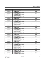
Page 145: ...4 DC DC Switching Regulators ...

Page 146: ...EATURES 0 9V Min operating voltage 10µA Typ maximum current consumption Standby operation 3µA Typ standby current consumption 1 05 0 05V high accuracy voltage detection Battery backup available on S1F76310 series On chip CR oscillator Power on clear available on S1F76310 and S1F76380 series Output voltage temperature characteristic for driving an LCD available on S1F76380 series SOP3 8pin APPLICAT...

Page 147: ...s Technical Manual BLOCK DIAGRAMS S1F76310 Series VI2 VI1 Reference voltage generator CR oscillator PWCR VSW VO GND RST PS Control switch S1F76380 Series RST PWCR VI VSW VO PS VCONT GND Reference voltage generator Control switch CR oscillator ...

Page 148: ...r on clear in the functional description 2 See standby mode and battery backup in the functional description PWCR GND VSW RST 1 3 4 2 8 6 5 7 PS VI2 VO VI1 S1F76310 series PWCR GND VSW RST 1 3 4 2 8 6 5 7 PS VCONT VO VI S1F76380 series S1F76380 Series Pin No Pin name Description 1 PWCR Power on clear See note 1 2 RST Reset signal output See note 1 3 GND Ground 4 VSW External inductor drive 5 VO Ou...

Page 149: ...ring must remain within the limits set out in LSI Device Precautions Never use solder dip to mount S1F70000 series power supply devices S1F76380 series Parameter Symbol Rating Unit Input voltage VI1 7 V Output current IO 100 mA Output voltage VO 7 V Power dissipation PD 200 SOP3 mW 300 DIP Operating temperature range Topr 30 to 85 C Storage temperature range Tstg 65 to 150 C Soldering temperature ...

Page 150: ... 0 9V VDS 0 2V 0 05 0 15 mA PS pull up current IIH VI1 1 5V 0 5 µA Multiplication clock frequency fCLK VI1 1 5V 30 40 50 kHz Electrical Characteristics S1F76310M1L0 VSS 0V Ta 25 C unless otherwise noted Parameter Symbol Condition Rating Unit Min Typ Max Input voltage VI1 VO VI2 0 9 1 8 V VI2 0 9 1 8 V Output voltage VO Vl1 1 5V 2 32 2 40 2 48 V Detection voltage VDET 1 00 1 05 1 10 V Detection vol...

Page 151: ...OL VI1 0 9V VDS 0 2V 0 05 0 15 mA PS pullup current IIH VI1 1 5V 0 5 µA Multiplication clock frequency fCLK VI1 1 5V 30 40 50 kHz S1F76310M1A0 VSS 0V Ta 25 C unless otherwise noted Parameter Symbol Condition Rating Unit Min Typ Max Input voltage VI1 VO VI2 0 9 2 0 V VI2 0 9 2 0 V Output voltage VO Vl1 1 5V 4 80 5 00 5 20 V Detection voltage VDET 1 00 1 05 1 10 V Detection voltage hysteresis ratio ...

Page 152: ...current IOL VI1 0 9V VOL 0 2V 0 05 0 15 mA PS pullup current IIH VI1 1 5V 0 5 µA Multiplication clock frequency fCLK VI1 1 5V 25 35 45 kHz S1F76380M1L0 VSS 0V Ta 25 C unless otherwise noted Parameter Symbol Condition Rating Unit Min Typ Max Input voltage VI1 0 9 2 0 V Output voltage VO Vl1 1 5V 2 30 2 40 2 50 V Output voltage temperature gradient Kt 5 5 4 0 3 5 mV C Detection voltage VDET 1 00 1 0...

Page 153: ...age temperature characteristic mV C Fixed output voltage temperature characteristic VI1 1 5 V 5 Standby current µA Ambient temperature C 4 3 2 1 0 0 25 75 50 85 30 1 15 1 10 1 05 1 00 0 95 30 0 25 85 VREL VDET 50 75 Ambient temperature C Detection voltage V 0 5 60 50 40 30 20 10 1 5 2 0 2 5 1 0 Input voltage V Clock frequency kHz Ta 25 C VI1 1 5 V 60 50 40 30 20 10 30 0 Ambient temperature C Clock...

Page 154: ...50 40 30 20 10 1 0 1 5 Input voltage V Clock frequency kHz 2 0 2 5 Ta 25 C 30 60 50 40 30 20 10 VI1 1 5 V 0 25 Ambient temperature C Clock frequency kHz 50 85 Clock frequency vs ambient temperature 30 2 5 2 0 0 25 Ambient temperature C Output Voltage V 50 85 75 S1F76310M1A0 Clock frequency vs ambient temperature 60 50 40 30 Clock frequency kHz 10 2 5 2 0 1 5 Input voltage V 1 0 0 5 20 Ta 25 C 60 5...

Page 155: ...C fCLK 32 kHz 100 10 100 50 0 5 Maximum load current mA Load efficiency 0 200 300 Inductence µH 500 1000 Ta 25 C fCLK 32 kHz ILmax Peff S1F76310M1B0 Notes 1 VI1 1 5V 2 Inductor TDK NLF453232 series Diode Shindengen DINS4 Schottky barrier diode Capacitor NEC MSUB20J106M 10µF Notes Inductor TDK NLF453232 221k 220µH Diode Shindengen DINS4 Schottky barrier diode Capacitor NEC MSUB20J106M 10µF 4 0 3 5 ...

Page 156: ...diode Capacitor NEC MSUB20J106M 10µF 4 0 3 5 3 0 2 5 2 0 1 5 1 0 0 10 Load current mA Output voltage V 5 15 20 25 VI 1 0 V V 1 5 V V 1 25 V fCLK 35 kHz 4 0 3 5 3 0 2 5 2 0 1 5 1 0 0 10 Load current mA Output voltage V 5 15 20 25 VI1 1 0 V VI1 1 5 V VI1 1 25 V fCLK 35 kHz 15 10 5 0 0 50 100 100 200 300 Inductance µH Maximum load current mA Load efficiency 500 1000 Ta 25 C fCLK 40 kHz ILmax Peff Not...

Page 157: ...0 100 50 0 0 1 0 5 1 0 0 6 0 8 0 2 0 3 C µF t pd msec 0 7 0 4 R 200 kΩ R 100 kΩ S1F76310M1B0 S1F76310M1L0 and S1F76380M1L0 S1F76380M1H0 200 150 100 50 0 C µF 0 1 0 2 1 0 0 8 0 7 0 6 0 5 0 3 0 4 t pd msec R 200 kΩ R 100 kΩ 200 150 100 50 0 C µF 0 1 0 2 1 0 0 8 0 7 0 6 0 5 0 3 0 4 t pd msec R 200 kΩ R 100 kΩ 200 150 100 50 0 C µF 0 1 0 2 1 0 0 8 0 7 0 6 0 5 0 3 0 4 t pd msec R 200 kΩ R 100 kΩ ...

Page 158: ...hen it is off this energy flows through D to change C Internal Circuits CR oscillator The S1F76310 S1F76380 series use a built in CR os cillator to drive the voltage booster circuit The circuit is supplied by VI1 All circuit components are on chip and thus the drive frequency is set internally To ensure 50 duty this frequency is twice that used by the volt age booster circuit When PS is Low the os...

Page 159: ...e the func tion If VI1 drops below VDET Tr1 and Tr2 conduct and PWCR and RST are grounded If VI1 recovers and rises higher than VREL Tr1 turns OFF The detection volt age hysteresis is 5 Typ and VREL is VDET 1 05 Typ VO returns to its normal value when the voltage of PWCR increases and Tr2 turns OFF so that RST re turns to VO after a delay specified by the time coeffi cient of R1 and C1 Thus after ...

Page 160: ...sed to drive the inductor is turned OFF and the built in backup switch is turned ON so that the input voltage at VI2 is output at VO This enables the battery backup function PS is pulled up internally so when standby mode is not required the pin should be left open Powering up Ensure that VO is at least the minimum operating volt age 0 9V before switching on the booster circuit One way to do this ...

Page 161: ...VF Capacitor To minimize ripple voltages use a capacitor with a small equivalent direct current resistance for smooth ing Notes 100µH L 1mH C 10µF D Schottky diode S1F76310M1A0 Peff 70 when L 220µH leadless inductor VI1 1 5V fCLK 32kHz IO 4mA Peff 75 when L 220µH drum coil VI1 1 5V fCLK 32kHz IO 6mA Peff 80 when L 300µH toroidal coil VI1 1 5V fCLK 32kHz IO 7mA S1F76310M1B0 Peff 70 when L 220µH lea...

Page 162: ...NLF453232 121K 120 0 10 50 0 796 8 3 64 30 NLF453232 151K 150 0 10 50 0 796 7 4 16 28 NLF453232 181K 180 0 10 40 0 796 6 5 72 26 NLF453232 221K 220 0 10 40 0 796 5 5 6 30 24 NLF453232 271K 270 0 10 40 0 796 5 6 90 23 NLF453232 331K 330 0 10 40 0 796 4 5 7 54 23 NLF453232 391K 390 0 10 40 0 796 4 8 20 21 NLF453232 471K 470 0 10 40 0 796 3 8 9 20 19 NLF453232 561K 560 0 10 40 0 796 3 6 10 50 18 NLF4...

Page 163: ...H 35 to 110 Device Rated current IDC Inductance µH at 20kHz 5V Diameter height Wire gauge A IDC 0 IDC rating mm Max mmø HP011 1 200 160 0 5 HP021 2 65 55 φ 20 12 0 7 HP031 3 30 23 0 8 HP012 1 600 450 0 5 HP022 2 180 135 φ 22 13 0 7 HP032 3 120 80 0 8 HP052 5 45 30 1 0 HP013 1 1000 800 0 5 HP023 2 500 330 φ 26 14 0 7 HP033 3 130 100 0 8 HP055 5 90 55 1 0 HP034S 3 400 250 0 8 HP054S 5 350 160 φ 36 1...

Page 164: ... Static capacitance Tan δ Leakage Device type voltage V µF 25 85 125 55 current µA C C C MSVAOJ475M A 6 3 4 7 0 08 0 1 0 12 0 5 MSVB2OJ106M B2 6 3 10 0 08 0 1 0 12 0 6 MSVB2OJ156M B2 6 3 15 0 08 0 1 0 12 0 9 MSVBOJ156M B 6 3 15 0 08 0 1 0 12 0 9 MSVCOJ336M C 6 3 33 0 08 0 1 0 12 2 0 MSVD2OJ686M D2 6 3 68 0 08 0 1 0 12 4 2 MSVDOJ686M D 6 3 68 0 08 0 1 0 12 4 2 Note The figures on the previous pages...

Page 165: ...re Although the circuit appears to have two ON OFF con trol points PS on the S1F76310M1A0 and POFF on the S1F76610C M PS only shuts down the S1F76310M1A0 The input voltage still reaches the S1F76610C M through L and D C1 C1 10 µF C3 10µF C2 10 µF VO VSW L D VI1 VI 5 V VO 15V ROSC 1 MΩ POFF VI2 GND PS PWCR S1F76310M S1F76610C M 1 2 3 4 5 6 7 14 13 12 11 10 9 8 S1F76610C M VDD 5 V VDD 0 V VO 10 V VO...

Page 166: ...ure summarizes the relevant circuits inside an S1F76300 series chip VO is connected to the level shift and buffer circuit which provide the gate bias for the switching transistor driving the inductor The current drain IO1 varies with the load and is typically 10µA The current IO2 through the internal resistors R1 and R2 is typically 1µA VI VO IO CL IO IR IR RB RA C GND VSW Voltage adjustment circu...

Page 167: ...t age generators and transistors for driving an internal comparator They feature low power consumption low operating voltages and standby operation The devices offer a range of fixed output voltages from 2 35 to 5 00V They are available in 8 pin SOP3s FEATURES 0 9V Min operating voltage 8µA Typ maximum current consumption Standby operation 3µA Typ standby current consumption Built in oscillator ci...

Page 168: ... 4 VSW External inductor drive 5 VO Output voltage 6 CLO Oscillator output 7 VI Step up input voltage 8 PS Power save See note Note See standby mode in the functional description BLOCK DIAGRAMS S1F76330 series PIN ASSIGNMENTS S1F76330 series GND VO VSW CLO PS CI CO VI1 Reference voltage generator Control switch Oscillator 1 2 3 4 CO CI GND VSW S1F76330 series PS VI1 CLO VO 8 7 6 5 ...

Page 169: ...evices Electrical Characteristics S1F76330M1B0 VSS 0V Ta 25 C unless otherwise noted Parameter Symbol Conditions Rating Unit Min Typ Max Input voltage VI1 VO VI2 0 9 2 0 V Output voltage VO VI1 1 5V 2 90 3 00 3 10 V VI1 1 5V Operating current IDDO fCLK 32kHz 5 30 µA IO 1 0mA Standby current IDDS VI1 1 5V 3 10 µA Switching transistor ON resistance RSWON VI1 1 5V VO 3 0V 6 12 Ω VSW 0 2V Switching tr...

Page 170: ... 4 3 2 1 0 30 0 25 50 85 75 Input voltage V Normalized frequency deviation ppm 10 5 0 5 10 0 5 1 0 1 5 2 0 2 5 Normalized frequency deviation f f CG CD 20 pF CG CD 10 pF RD 200 kΩ VI 1 5 V fO 32 kHz Gate capacitance pF Normalized frequency deviation ppm 50 0 50 0 10 20 30 RD 200 kΩ VI 1 5 V fO 32 kHz CD 20 pF CD 10 pF Normalized frequency deviation f fO fO Normalized frequency deviation f f Input ...

Page 171: ... Shindengen DINS4 Schottky barrier diode Capacitor NEC MSVB20J106M 10µF 4 0 3 5 3 0 2 5 2 0 1 5 1 0 0 5 10 15 20 25 Load current mA Output voltage V fCLK 32 8 kHz VI1 1 0 V VI1 1 25 V VI1 1 5 V 100 200 300 500 1000 Inductance µH 10 5 0 100 50 0 Maximum load current mA Load efficiency Ta 25 C fCLK 32 kHz Peff ILmax PACKAGE MARKINGS S1F76330 device packages use the following marking 7 6 3 1 Series n...

Page 172: ...r output cannot be obtained without a voltage at VO Since the crystal oscillator is activated when an input voltage is applied oscillation continues even in standby mode Reference voltage generator and output voltage regulator The reference voltage generator regulates VI1 to gener ate a voltage for the voltage regulator circuit S1F76330 CI CO RD Crystal CD CG Note In step up voltage operation the ...

Page 173: ...iminate magnetic field leakage reduce losses and improve performance tors such as the switching frequency type of coil and the size and type of other external components S1F76330 series TYPICAL APPLICATIONS Example Circuits The output current IO and power conversion efficiency Peff of a particular device in the series depends on fac Notes 100µH L 1mH C 10µF D Schottky diode S1F76330M1B0 Peff 70 wh...

Page 174: ...10 50 2 52 10 2 60 36 NLF453232 820K 82 0 10 50 2 52 10 2 86 34 NLF453232 101K 100 0 10 50 0 796 9 3 25 32 NLF453232 121K 120 0 10 50 0 796 8 3 64 30 NLF453232 151K 150 0 10 50 0 796 7 4 16 28 NLF453232 181K 180 0 10 40 0 796 6 5 72 26 NLF453232 221K 220 0 10 40 0 796 5 5 6 30 24 NLF453232 271K 270 0 10 40 0 796 5 6 90 23 NLF453232 331K 330 0 10 40 0 796 4 5 7 54 23 NLF453232 391K 390 0 10 40 0 79...

Page 175: ... HP021 2 65 55 20 12 0 7 HP031 3 30 23 0 8 HP012 1 600 450 0 5 HP022 2 180 135 22 13 0 7 HP032 3 120 80 0 8 HP052 5 45 30 1 0 HP013 1 1000 800 0 5 HP023 2 500 330 26 14 0 7 HP033 3 130 100 0 8 HP055 5 90 55 1 0 HP034S 3 400 250 0 8 HP054S 5 350 160 36 14 1 0 HP104S 10 50 30 1 6 HP024 2 1500 950 0 7 HP034 3 300 230 36 21 0 8 HP054 5 210 140 1 0 HP104 10 45 30 1 6 HP035 3 700 500 0 8 HP055 5 600 330...

Page 176: ...0 1 0 12 0 5 MSVB20J106M B2 6 3 10 0 08 0 1 0 12 0 6 MSVB20J156M B2 6 3 15 0 08 0 1 0 12 0 9 MSVB0J156M B 6 3 15 0 08 0 1 0 12 0 9 MSVC0J336M C 6 3 33 0 08 0 1 0 12 2 0 MSVD20J686M D2 6 3 68 0 08 0 1 0 12 4 2 MSVD0J686M D 6 3 68 0 08 0 1 0 12 4 2 Note The figures on the previous pages show data from the documents of various manufacturers For further details please contact the relevant manufacturer...

Page 177: ...ure Although the circuit appears to have two ON OFF con trol points PS on the S1F76330M1B0 and POFF on the S1F76610C M PS only shuts down the S1F76330M1B0 The input voltage still reaches the S1F76610C M through L and D C C1 10 µF C3 10 µF C2 10 µF VO VSW L D VI1 VI 5 V VO 15 V ROSC 1 MΩ POFF GND PS CG CD RD S1F76330M S1F76610C M 1 2 3 4 5 6 7 14 13 12 11 10 9 8 S1F76610C M VDD 5 V VDD 0 V VO 10 V ...

Page 178: ...re summarizes the relevant circuits inside an S1F70000 series chip VO is connected to the level shift and buffer circuit which provide the gate bias for the switching transistor driving the inductor The current drain IO1 varies with the load and is typically 10µA The current IO2 through the internal resistors R1 and R2 is typically 1µA VI VO IO CL IO IR IR RB RA C GND VSW Voltage adjustment circui...

Page 179: ... a soft start protection circuit When receiving external sig nals S1F71100 can stop the oscillator and the switching circuit and turn off the power so that it can reduce wasteful current consumption at the time of system halt FEATURES Input voltage 3 3V 12V Output voltage 3 3V S1F71100M0A0 Power off current 1µA Self current consumption 800µA Frequency fixing 200kHz PWM Power off function IC shutdo...

Page 180: ...onnection pin for setting soft start and the VSS pin 2 POFFX Power off control pin During normal operation VDD level At power off time VSS level 3 VDD Power Power supply pin supply 4 ISENSE Load current feedback pin Load current detection resistor connection pin Connect a resistor of 100mΩ 5 SWO Output Switching Pch power MOS transistor drive pin 6 ERCAP Capacitor connection pin for external phase...

Page 181: ... time when the power is turned on Figure 6 1 The SSCAP pin is at the VSS level when the power is turned off When the soft start operation begins the soft start capacitor starts being charged and the voltage at the SSCAP pin rises slowly The output voltage rises gradually as the voltage at the SSCAP pin rises This operation controls the switching pulse width at the time when the power is turned on ...

Page 182: ... SSCAP pin SSCAP SSCAP VSS 0 3 to VDD 0 3 V Voltage at SWO pin SWO SWO VSS 0 3 to VDD 0 3 V Voltage at ISENSE pin ISENSE ISENSE VSS 0 3 to VDD 0 3 V Package allowable loss PD PD 300 MW Ta 25 C Operating temperature Topr 30 to 85 C Storage temperature Tstg 55 to 150 C Soldering temperature and time Tsol 260 10 C S Note Any operation under conditions exceeding the above absolute maximum ratings may ...

Page 183: ... VO VDD 5 0 to 10v 30 mV Load stability VO IO 10mA to 300mA 30 mV Soft start time TSS Capacitance for SS 0 1µF 40 ms VDD 5 0V IO 300mA Input voltage VIH 0 8VDD V at POFFX pin VIL 0 2VDD V Leak current ILINH VI VDD 0 1 µA at POFFX pin ILINL VI VSS 0 1 µA Conversion efficiency EFFI VDD 5 0V 90 IO 200mA Oscillation frequency fOSC VDD 5 0V VO VSS 150 200 250 kHz SWO pin Overcurrent detection IDET VDD ...

Page 184: ...tection circuit Error amplifier Driver Overcurrent protection circuit Load current detection resistor R Pch MOSTr D CVOUT VO 3 3V L PWM circuit Soft start Oscillator Reference voltage circuit Parts examples CIN1 100µF Sanyo 16SA100M CIN2 1µF SSCAP 0 1µF ERCAP 330pF R 100mΩ PchTr Hitachi 2SJ484 L 47µH Sumida CD105 CVO 47µF Sanyo 16SA47M D Schottkey Rohm RB161L 40 Characteristics vary with applicabl...

Page 185: ...ax Min Nom Max E 4 8 5 5 2 0 189 0 197 0 204 D1 A 1 75 0 069 A1 0 15 0 006 A2 1 6 0 063 e 1 27 0 05 b 0 25 0 35 0 45 0 010 0 014 0 017 C 0 05 0 15 0 25 0 002 0 006 0 009 θ L 0 55 0 022 L1 L2 HE 6 4 6 8 7 2 0 252 0 268 0 283 D 4 8 5 5 2 0 189 0 197 0 204 θ2 θ3 R R1 for reference 8 5 1 4 INDEX D E H E θ e b A 1 A 2 A θ3 θ2 L C R R1 L1 L2 Reference Plastic SOP4 8pin ...

Page 186: ...ulation system PWM when the input voltage is Low S1F71200 is also provided with an overcurrent protec tion circuit and a soft start circuit When receiving ex ternal signals S1F71200 can stop the oscillator and the switching circuit and turn off the power so that it can reduce wasteful current consumption at the time of sys tem halt FEATURES Input voltage 2 5V to 12 0V Output voltage 5 0V S1F71200M...

Page 187: ...00 Series Technical Manual BLOCK DIAGRAM SWO VDD1 VDD2 EXO VO SRC IREF VREF SSC VSS SWC VC POFFX VSW ISENSE Oscillator PWM _ _ _ Driver Overcurrent detection circuit Soft start Series regulator Error amplifier Reference voltage circuit ...

Page 188: ...S1F71200 Series S1F70000 Series EPSON 4 43 Technical Manual S1F71200 Series PIN ASSIGNMENTS 1 2 3 4 5 6 7 8 16 15 14 13 12 11 10 9 Index SSOP2 16pin ...

Page 189: ...regulator Step up step down output feedback pin Series regulator phase compensation capaci tor connection pin Reference resistor connection pin Connect a 100kΩ resistor between the VSS pins Reference voltage pin Connect a 0 1µF capacitance between the VSS pins No connection Power off control pin During normal operation POFFX VDD1 At power off time POFFX VSS Step up output voltage setting pin For s...

Page 190: ...200 reduces the on duty for control When voltages higher than the step up set voltage is constantly supplied to the VSW pin S1F71200 stops operation of the step up switching When the switching stops completely the input voltage is supplied to the VSW pin through the coil and the di ode The voltage at the VSW pin comes to the one ob tained by reducing VF of the diode from the input volt age Step up...

Page 191: ... transistor as an external part S1F71200 reduces voltage supplied to the VDD2 pin and constitutes a series regulator The VDD2 pin is generally connected to the VSW pin of step up output This series regulator operates monitoring voltage at the VO pin of step up step down output It controls the drive current base current of the PNP transistor at the EXO pin to stabilize voltage at the VO pin Power O...

Page 192: ...a 25 C 30 to 85 55 to 150 260 10 Unit V V V V V V V V V V V V V MW C C C s Note Any operation under conditions exceeding the above absolute maximum ratings may result in a malfunction or a permanent destruction When even an item is more than the rating a temporary normal operation is possible but with remarkably low reliability So be sure to keep all items below the ratings Parameter Input voltage...

Page 193: ... current at SWO pin Input stability Load stability Input voltage level at POFFX pin at VC pin Symbol VDD1 VDD2 VSW VO IVDD1 1 VDD1 system IVDD2 1 VDD2 system IVDD1 2 VDD1 system IVDD2 2 VDD2 system IQ IOHSWO IOLSWO VO VO VIH VIL Conditions VDD1 pin VDD2 pin VSW1 pin VC VDD1 VC VSS VDD2 6V Ta 30 C to 85 C VDD1 3V VDD2 6V VDD1 3V VDD2 6V VDD1 6V VDD2 6V VDD1 6V VDD2 6V VDD1 12V VDD2 12V VDD1 3V VDD2...

Page 194: ...5 200 0 15 0 015 Max 1 0 1 0 280 0 20 Parameter Input pin leak current at POFFX pin at VC pin Step up soft start time Step up portion conversion efficiency Oscillation frequency Overcurrent detection voltage Output voltage temperature coefficient Symbol ILINH ILINL TSS EFFI fOSC IDET VO Topr Conditions VIN VDD1 VIN VSS SSCAP 0 1µF VDD1 3 0V VC VDD1 IO 50mA VDD1 3 3V VC VSS VDD1 3V Measure it at th...

Page 195: ... time current consumption 2 operation for step down only Power off time current consumption Output current at SWO pin Input stability Load stability Input voltage level at POFFX pin at VC pin Symbol VDD1 VDD2 VSW VO IVDD1 1 VDD1 system IVDD2 1 VDD2 system IVDD1 2 VDD1 system IVDD2 2 VDD2 system IQ IOHSWO IOLSWO VO VO VIH VIL Conditions VDD1 pin VDD2 pin VSW1 pin VC VDD1 VC VSS VDD2 4 3V Ta 30 C to...

Page 196: ... Typ 70 85 200 0 15 0 015 Max 1 0 1 0 280 0 20 Parameter Input pin leak current at POFFX pin at VC pin Step up soft start time Step up portion conversion efficiency Oscillation frequency Overcurrent detection voltage Output voltage temperature coefficient Symbol ILINH ILINL TSS EFFI fOSC IDET VO Topr Conditions VIN VDD1 VIN VSS SSCAP 0 1µF VDD1 3 0V VC VDD1 IO 50mA VDD1 3V VC VSS VDD 3V Measure it...

Page 197: ...ERNAL CONNECTION OF REFERENCE CIRCUIT Basic Circuit SWO VDD1 VDD2 EXO VO SRC IREF VREF SSC VSS SWC VC POFFX VSW ISENSE PWM _ _ _ Oscillator Driver Overcurrent detection circuit Soft start Series regulator Error amplifier Reference voltage circuit Input voltage Output voltage ...

Page 198: ... CSSC VSS SWC VC POFFX VSW ISENSE RSENSE Nch MOSTr Input voltage Output voltage Parts examples CVDD1 47µF Sanyo 16SA47M NchTr Hitachi HAT2037T L 47µH Sumida CR54 D Schottky Rohm RB161L 40 CVSW 47µF Sanyo 16SA47M PNPTr 2SA1242 CVOUT 22µF Sanyo 10SL22M RIREF 100kΩ CVREF 0 1µF CSSC 0 1µF RSENSE 0 1Ω Characteristics vary with applicable conditions and parts Select proper parts after sufficient evaluat...

Page 199: ...C θ L L1 L2 HE D θ2 θ3 R R1 Min 4 2 6 4 1 4 0 26 0 1 0 0 3 5 9 Nom 4 4 6 6 0 05 1 5 0 8 0 36 0 15 0 5 0 9 0 4 6 2 Max 4 6 6 8 1 7 1 6 0 46 0 25 10 0 7 6 5 7 Min 0 166 0 252 0 056 0 011 0 004 0 0 012 0 233 Nom 0 173 0 260 0 002 0 059 0 031 0 014 0 006 0 020 0 035 0 016 0 244 Max 0 181 0 267 0 066 0 062 0 018 0 009 10 0 027 0 255 0 275 Dimension in Milimeters Dimension in Inches Lead type STD SSOP2 ...

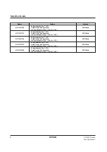
Page 200: ...5 Voltage Detector ...

Page 201: ...ploys N channel open drain output approach And the S1F77210Y series and S1F 77220Y series employ the CMOS output and P channel output respectively The package used is the SOT89 3 pin plastic package Our voltage detectors are used for determining battery life and also for monitoring supply voltage fed to mi crocomputers and LSI systems FEATURES Full lineups 19 types are prepared for the detection r...

Page 202: ...vel S1F77210Y1J0 4 30 4 40 4 50 CMOS Low level High level S1F77210Y120 4 50 4 60 4 70 CMOS Low level High level S1F77210Y1K0 4 70 4 80 4 90 CMOS Low level High level S1F77210Y1L0 4 90 5 00 5 10 CMOS Low level High level S1F77210Y2C0 2 10 2 15 2 20 CMOS High level Low level S1F77210Y2F0 2 60 2 65 2 70 CMOS High level Low level Product Voltage detectable Output type Output phase Min Typ Max Less tha...

Page 203: ...7220Y1 0 Type S1F77220Y2 0 Type Note A different code can be employed for the ones preceded by marking depending on their detecting voltage specification VDD 2pin OUT 1pin T VSS 3pin T VREF VDD 2pin OUT 1pin T VSS 3pin T VREF VDD 2pin OUT 1pin T VSS 3pin T VREF VDD 2pin OUT 1pin T VSS 3pin T VREF VDD 2pin OUT 1pin T VSS 3pin T VREF VDD 2pin OUT 1pin T VSS 3pin T VREF ...

Page 204: ...ply and the reference voltage VREF gener ated on the IC are entered to the voltage comparator Since the voltage comparator is designed to detect a tar get voltage even when potential difference between VREG and Vref minute hysteresis is added so that the comparator may not fail due to noise on the power sup ply and such In the example shown in the figure below detection voltage VDET for the input ...

Page 205: ...f the OUT terminal may become unsteady Ensure to prevent problems from occurring in circuit operation ABSOLUTE MAXIMUM RATINGS OUT 0 0 VDD V1 VHYS VDET Detection voltage VREL Relief voltage VREL VDET Operating voltage upper limit Operating voltage lower limit OUT 0 0 VDD V1 VHYS VDET Detection voltage VREL Relief voltage VREL VDET Operating voltage upper limit Operating voltage lower limit Paramet...

Page 206: ...tput current IOL VDD 2 0V 0 20 1 00 mA OUT 0 2V VDD 3V 2V 8 40 µs Detection voltage TPHL Ta 25 C response time VDD 3V 2V 200 µs Ta 30 C to 85 C S1F77210Y1C0 Ta 30 C to 85 C is assumed except where otherwise specified Parameter Symbol Conditions VSS 0 0V Min Typ Max Unit Operating voltage VDD 1 50 12 0 V Detection voltage VDET Ta 25 C 2 10 2 15 2 20 V Hysteresis width VHYS VHYS VREL VDET 0 05 0 10 ...

Page 207: ... current IOL VDD 2 0V 0 20 1 00 mA OUT 0 2V VDD 3V 2V 8 40 µs Detection voltage TPHL Ta 25 C response time VDD 3V 2V 200 µs Ta 30 C to 85 C S1F77210Y1E0 Ta 30 C to 85 C is assumed except where otherwise specified Parameter Symbol Conditions VSS 0 0V Min Typ Max Unit Operating voltage VDD 1 50 12 0 V Detection voltage VDET Ta 25 C 2 50 2 55 2 60 V Hysteresis width VHYS VHYS VREL VDET 0 05 0 10 0 15...

Page 208: ...IOL VDD 2 0V 0 20 1 00 mA OUT 0 2V VDD 3V 2V 8 40 µs Detection voltage TPHL Ta 25 C response time VDD 3V 2V 200 µs Ta 30 C to 85 C S1F77210Y1R0 Ta 30 C to 85 C is assumed except where otherwise specified Parameter Symbol Conditions VSS 0 0V Min Typ Max Unit Operating voltage VDD 1 50 12 0 V Detection voltage VDET Ta 25 C 2 73 2 80 2 87 V Hysteresis width VHYS VHYS VREL VDET 0 05 0 10 0 15 V Operat...

Page 209: ... current IOL VDD 2 0V 0 20 1 00 mA OUT 0 2V VDD 4V 3V 8 40 µs Detection voltage TPHL Ta 25 C response time VDD 4V 3V 200 µs Ta 30 C to 85 C S1F77210Y1H0 Ta 30 C to 85 C is assumed except where otherwise specified Parameter Symbol Conditions VSS 0 0V Min Typ Max Unit Operating voltage VDD 1 50 12 0 V Detection voltage VDET Ta 25 C 3 13 3 20 3 27 V Hysteresis width VHYS VHYS VREL VDET 0 09 0 15 0 21...

Page 210: ... IOL VDD 2 0V 0 20 1 00 mA OUT 0 2V VDD 4V 3V 8 40 µs Detection voltage TPHL Ta 25 C response time VDD 4V 3V 200 µs Ta 30 C to 85 C S1F77210Y1T0 Ta 30 C to 85 C is assumed except where otherwise specified Parameter Symbol Conditions VSS 0 0V Min Typ Max Unit Operating voltage VDD 1 50 12 0 V Detection voltage VDET Ta 25 C 3 90 4 00 4 10 V Hysteresis width VHYS VHYS VREL VDET 0 13 0 20 0 27 V Opera...

Page 211: ... current IOL VDD 2 0V 0 20 1 00 mA OUT 0 2V VDD 5V 4V 8 40 µs Detection voltage TPHL Ta 25 C response time VDD 5V 4V 200 µs Ta 30 C to 85 C S1F77210Y1J0 Ta 30 C to 85 C is assumed except where otherwise specified Parameter Symbol Conditions VSS 0 0V Min Typ Max Unit Operating voltage VDD 1 50 12 0 V Detection voltage VDET Ta 25 C 4 30 4 40 4 50 V Hysteresis width VHYS VHYS VREL VDET 0 13 0 20 0 27...

Page 212: ... IOL VDD 2 0V 0 20 1 00 mA OUT 0 2V VDD 5V 4V 8 40 µs Detection voltage TPHL Ta 25 C response time VDD 5V 4V 200 µs Ta 30 C to 85 C S1F77210Y1K0 Ta 30 C to 85 C is assumed except where otherwise specified Parameter Symbol Conditions VSS 0 0V Min Typ Max Unit Operating voltage VDD 1 50 12 0 V Detection voltage VDET Ta 25 C 4 70 4 80 4 90 V Hysteresis width VHYS VHYS VREL VDET 0 13 0 20 0 27 V Opera...

Page 213: ... current IOL VDD 2 0V 0 20 1 00 mA OUT 0 2V VDD 6V 4V 8 40 µs Detection voltage TPHL Ta 25 C response time VDD 6V 4V 200 µs Ta 30 C to 85 C S1F77210Y1C0 Ta 30 C to 85 C is assumed except where otherwise specified Parameter Symbol Conditions VSS 0 0V Min Typ Max Unit Operating voltage VDD 1 50 12 0 V Detection voltage VDET Ta 25 C 2 10 2 15 2 20 V Hysteresis width VHYS VHYS VREL VDET 0 05 0 10 0 15...

Page 214: ... 1 8V Low level output current IOL VDD 3 0V 0 50 2 00 mA OUT 0 3V VDD 3V 2V 8 40 µs Detection voltage TPHL Ta 25 C response time VDD 3V 2V 200 µs Ta 30 C to 85 C S1F77200Y1T0 Ta 30 C to 85 C is assumed except where otherwise specified Parameter Symbol Conditions VSS 0 0V Min Typ Max Unit Operating voltage VDD 1 50 12 0 V Detection voltage VDET Ta 25 C 3 90 4 00 4 10 V Hysteresis width VHYS VHYS VR...

Page 215: ... current IOL VDD 2 0V 0 20 1 00 mA OUT 0 2V VDD 3V 2V 8 40 µs Detection voltage TPHL Ta 25 C response time VDD 3V 2V 200 µs Ta 30 C to 85 C S1F77200Y1C0 Ta 30 C to 85 C is assumed except where otherwise specified Parameter Symbol Conditions VSS 0 0V Min Typ Max Unit Operating voltage VDD 0 80 10 0 V Detection voltage VDET Ta 25 C 2 10 2 15 2 20 V Hysteresis width VHYS VHYS VREL VDET 0 05 0 10 0 15...

Page 216: ...VDD 1 5V 0 15 0 75 mA OUT 0 15V VDD 2V 1V 8 40 µs Detection voltage TPHL Ta 25 C response time VDD 2V 1V 200 µs Ta 30 C to 85 C S1F77200Y1B0 Ta 30 C to 85 C is assumed except where otherwise specified Parameter Symbol Conditions VSS 0 0V Min Typ Max Unit Operating voltage VDD 0 80 10 0 V Detection voltage VDET Ta 25 C 1 10 1 15 1 20 V Hysteresis width VHYS VHYS VREL VDET 0 03 0 05 0 08 V Operating...

Page 217: ...IOL VDD 0 8V 0 05 0 40 mA OUT 0 16V VDD 1 5V 0 8V 8 40 µs Detection voltage TPHL Ta 25 C response time VDD 1 5V 0 8V 200 µs Ta 30 C to 85 C S1F77200Y1A0 Ta 30 C to 85 C is assumed except where otherwise specified Parameter Symbol Conditions VSS 0 0V Min Typ Max Unit Operating voltage VDD 0 80 10 0 V Detection voltage VDET Ta 25 C 1 00 1 05 1 10 V Hysteresis width VHYS VHYS VREL VDET 0 03 0 05 0 08...

Page 218: ...0 8V 0 05 0 40 mA OUT 0 16V VDD 1 5V 0 8V 8 40 µs Detection voltage TPHL Ta 25 C response time VDD 1 5V 0 8V 200 µs Ta 30 C to 85 C S1F77220Y2D0 Ta 30 C to 85 C is assumed except where otherwise specified Parameter Symbol Conditions VSS 0 0V Min Typ Max Unit Operating voltage VDD 1 5 12 0 V Detection voltage VDET Ta 25 C 1 20 1 25 1 30 V Hysteresis width VHYS VHYS VREL VDET 0 03 0 05 0 08 V Operat...

Page 219: ...UT S1F77210Y Series Input voltage Input voltage Voltage detection output 3pin 2pin 1pin OUT Input voltage Input voltage Voltage detection output Power supply for pull up resistor VDD VSS S1F77210Y Series 3pin 2pin 1pin OUT Power supply for pull down resistor Input voltage Input voltage Voltage detection output VDD VSS S1F77210Y Series ...

Page 220: ...it can be used as a CR timer circuit Figure 5 14 CR timer circuit Battery backup circuit The following is an example of the supply voltage switching circuit for the battery backup supply configured featur ing the S1F77210Y series Figure 5 15 Battery backup circuit VDD VDD VO VSS OUT R C S1F77210Y VDD VCC VBAT VDD VO VSS PNP transistor NPN transistor Enable signal S1F77210Y ...

Page 221: ...Figure 5 16 it can be used as a CR timer circuit Figure 5 16 CR timer circuit Battery backup circuit The following is an example of the supply voltage switching circuit for the battery backup configured featuring the S1F77200Y series Figure 5 17 Battery backup circuit VDD VCC VBAT VDD VO VSS PNP transistor NPN transistor Enable signal S1F77200Y VDD VDD VDD VO VSS OUT R C S1F77200Y ...

Page 222: ...re not check for short cut current after volume production has been started Although duration of the short cut current depends on operating conditions such as type the circuit used and supply impedance normally it is assumed to continue several usec to several dozens of usec If a load with high impedance is inserted across the power supply oscillation can be introduced by the short cut current In ...

Page 223: ...6 Appendix ...

Page 224: ...nge for device storage with no degradation or damage This specification is par ticularly important when ICs are being transported by air 7 Soldering temperature and the duration The maximum soldering temperature and the time for which the leads can be at this temperature RECOMMENDED OPERATING CONDITIONS Recommended operating conditions are the conditions under which a device functions correctly Th...

Page 225: ...acitance CT Crosstalk CTn Temperature gradient fCLK Clock frequency fmax Maximum clock frequency fOSC Oscillator frequency FT Field through channel OFF IBSQ Backup switching leakage current IDDO Operating current IDDS Standby current IDD Power supply current IIH High level input current IIL Low level input current ILKI input leakage current IMAX Maximum current IO Output current IOH High level out...

Page 226: ...utput voltage regulated VSS Power supply voltage VSSn Power supply voltage VSTA Oscillator start up voltage VSTP Oscillator shut down voltage Symbol Parameter tMR Memory reset Topr Operating temperature tPAE Propagation delay tPHL Low level transition time tPLH High level transition time tPLS Propagation delay tPOP Propagation delay tPS Propagation delay tSA Address setup time tSD Data setup time ...

Page 227: ...54 0 25 7 62 7 62 to 9 02 0 25 0 03 0 01 INDEX 14 0 1 19 6 0 4 20 0 1 25 48 0 35 0 1 24 1 2 7 0 1 2 8 1 5 0 3 0 15 0 05 0 8 14 8 1 7 19 7Max 19 0 0 1 6 3 0 1 1 5 0 46 0 1 2 54 0 25 7 62 to 9 02 7 62 0 25 0 03 0 01 0 8 0 1 3 0 Min 4 4 0 1 7 0 0 1 9 0 0 4 25 36 7 0 0 1 9 0 0 4 13 24 INDEX 0 18 0 1 12 1 48 37 1 7 Max 1 0 0 5 0 2 0 125 0 05 0 5 5 8 4 1 INDEX 1 27 5 0 0 2 6 0 0 4 3 9 0 2 0 4 0 1 1 5 0 ...

Page 228: ... 3 2 3 10 5Max 0 1 0 08 13 24 12 1 1 27 15 2 0 1 8 4 0 1 0 4 0 1 2 7 2 5 0 15 0 15 0 05 15 5Max 11 8 0 3 0 2 1 0 9 16 8 1 INDEX 4 4 0 2 1 7 Max 0 05 0 9 0 15 6 8 0 2 6 6 0 2 6 2 0 3 1 5 0 5 0 2 0 10 0 8 0 36 0 1 1 8Max 4 5 0 1 2 5 0 1 4 25 Max 1 5 0 48Max 1 2 3 1 5 0 4 0 8 Min 0 48Max 0 53Max 1 5 0 1 0 44Max 0 44Max 15 28 14 1 1 27 17 8 0 1 8 4 0 1 0 4 0 1 2 7 0 2 0 15 0 05 18 1Max 11 8 0 3 2 5 0 ...

Page 229: ...5 T 0 3 T2 2 3 W 12 0 0 2 W1 9 5 θ 30 Max There are no joints in either the cover or carrier tapes Less than 0 2 of the total device count is comprised of non sequential blanks There are no sequential blanks This does not apply to the tape leader and trailer Note The tape thickness is 0 1 mm Max the EIAJ RCI00B electronic parts taping specification Each tape holds 1 000 devices Device cavity T2 T ...

Page 230: ... W 14 0 See note W1 1 5 0 1 W2 17 See note r 1 0 REEL SPECIFICATIONS The reel specifications are shown in the following table and figure The reel is made of paperboard Note W and W2 are measured at the reel core DEVICE POSITIONING Small molded power IC devices are positioned as shown in the following figure 120 120 E C D r W W1 W2 B A T1 T2 ...

Page 231: ...05 T2 2 5 W 12 0 0 3 W1 9 5 θ 15 Max blanks This does not apply to the tape leader and trailer Dimension code Dimensions angles mm A 6 7 B 5 4 D 1 55 0 05 0 D1 1 55 0 05 E 1 75 0 1 F 5 5 0 1 P1 8 0 0 1 P0 4 0 0 1 Note The tape thickness is 0 1 mm Max There are no joints in either the cover or carrier tapes Less than 0 2 of the total device count is comprised of non sequential blanks There are no s...

Page 232: ... Dimension code Dimensions mm A 330 2 0 B 80 1 0 C 13 0 0 5 D 21 0 0 5 E 2 0 0 5 W 15 4 1 0 See note W1 2 0 0 5 W2 23 4 See note r 1 0 Note W and W2 are measured at the reel core DEVICE POSITIONING Type B products are positioned so that the index mark is on the sprocket hole side of the tape as shown in the following figure 120 120 E C D r W W1 W2 B A Index mark Travel direction ...

Page 233: ...EPSON S1F70000 Series Technical Manual Appendix Type F product are positioned so that the index mark is on the opposite side to the sprocket holes as shown in the following figure Index mark Travel direction ...

Page 234: ...ape leader and trailer Dimension code Dimensions mm A 8 4 B 10 6 D0 1 55 0 05 D1 1 55 0 05 E 1 75 0 1 F 7 5 0 1 P1 12 0 1 P0 4 0 0 1 Note The tape thickness is 0 1 mm Max There are no joints in either the cover or carrier tapes Less than 0 1 of the total device count is comprised of non sequential blanks There are no sequential the EIAJ RCI009B electronic parts taping specification Each tape holds...

Page 235: ...W and W2 are measured at the reel core DEVICE POSITIONING Type B products are positioned so that the index mark is on the sprocket hole side of the tape as shown in the following figure Dimension code Dimensions mm A 330 2 0 B 80 1 0 C 13 0 0 5 D 21 0 1 0 E 2 0 0 5 W 14 0 1 5 See note W1 2 0 0 5 W2 20 5 max See note r 1 0 120 120 E D r W W1 W2 B C A Index mark Travel direction ...

Page 236: ...eries EPSON 6 13 Technical Manual Appendix Appendix Type F products are positioned so that the index mark is on the opposite side to the sprocket holes as shown in the following figure Index mark Travel direction ...

Page 237: ... part name quantity and lot number Dimension code Dimensions mm A 12 4 B 15 6 D0 1 55 0 1 0 D1 2 0 0 1 0 E 1 75 0 1 F 11 5 0 1 P1 16 0 1 Note The tape thickness is 0 1 mm Max There are no joints in either the cover or carrier tapes Less than 0 2 of the total device count is comprised of non sequential blanks There are no sequential blanks This does not apply to the tape leader and the EIAJ RCI009B...

Page 238: ...ank sections are provided as a leader and trailer with 1 000 SOP2 packages fitted into the com ponent mounting section between them At the begin ning of the leader section there is an extra section of tape which contains the cover tape only Travel direction Base Embossed carrier Lead open 40mm Trailer open 40mm Cover tape only Finish Start ...

Page 239: ...e W and W2 are measured at the reel core DEVICE POSITIONING Type B products are positioned so that the index mark is on the sprocket hole side of the tape as shown in the following figure Dimension code Dimensions mm A 330 2 0 B 80 1 0 C 13 0 0 5 D 21 0 1 0 E 2 0 0 5 W 24 4 2 0 See note W1 2 0 0 5 W2 31 4 Max See note r 1 0 120 120 E D r W W1 W2 B C A Index mark Travel direction ...

Page 240: ...eries EPSON 6 17 Technical Manual Appendix Appendix Type F products are positioned so that the index mark is on the opposite side to the sprocket holes as shown in the following figure Index mark Travel direction ...

Page 241: ...ston West Lothian EH54 7EG SCOTLAND Phone 44 1506 605040 Fax 44 1506 605041 ASIA EPSON CHINA CO LTD 23F Beijing Silver Tower 2 North RD DongSanHuan ChaoYang District Beijing CHINA Phone 64106655 Fax 64107319 SHANGHAI BRANCH 4F Bldg 27 No 69 Gui Qing Road Caohejing Shanghai CHINA Phone 21 6485 5552 Fax 21 6485 0775 EPSON HONG KONG LTD 20 F Harbour Centre 25 Harbour Road Wanchai Hong Kong Phone 852 ...

Page 242: ...ty that anything made in accordance with this material will be free from any patent or copyright infringement of a third party This material or portions thereof may contain technology or the subject relating to strategic products under the control of the Foreign Exchange and Foreign Trade Low of Japan and may require an export licenes from the Ministry of International Trade and Industry or other ...

Page 243: ...nual S1F70000 Series EPSON Electronic Devices Website ELECTRONIC DEVICES MARKETING DIVISION First issue November 1990 U Revised July 2002 in Japan H B 4 5mm Technical Manual POWER SUPPLY IC S1F70000 Series http www epson co jp device This manual was made with recycle paper and printed using soy based inks ...

Reviews: