background image

4. CPUIF Verification Procedure 


12 

EPSON 

S1R72V17 CPU Connection Guide 

(Rev. 1.0)


6)  Clock input setting 

Write the clock input setting value to the ClkSelect register (0x73h address). 

This sets the clock input method and frequency used for the S1R72V17. The settings are shown in Table 
4-2. 

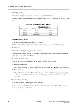
Table 4-2    ClkSelect register settings 


Clock input method 

Clock frequency 

External oscillator 

External clock source 

12 MHz 

0x00 

0x80 

24 MHz 

0x01 

0x81 

48 MHz 

Not available 

0x83 


7)  Clock input setting protect 

Write 0x00 to the ModeProtect register (0x071 address). 

Writing a value other than 0x56 to this register enables write protection for the ClkSelect register. 

8) MTM 

reset 

Write 0x00 to the ChipReset register (0x011 address). 

Clearing the bit7 ResetMTM bit to “0” clears the USB Transceiver Macro reset and enables oscillation 
of the PLL contained in the S1R72V17. 

9)  Oscillation start time setting 

Write the oscillation start time to the WakeupTim_H,L registers (0x014 address). 

With external clock source: 

Write 0x0010. Note that the external clock source oscillation must have stabilized before this occurs. 

With external oscillator: 

The standard time is usually within the clock frequency ±10%, but this will vary greatly, depending 
on the selected oscillator, circuit board, and external components. Write 0x2500 here to check the 
connection. 

10)  Internal clock feed setting 

Write 0x40 to the PM_Control register (0x012 address). 

Setting the bit6 GoActive bit to “1” starts the internal clock operation (starts OSC and PLL) and starts 
the clock feed to the internal circuit. 

Summary of Contents for S1R72V17

Page 1: ...Rev 1 0 S1R72V17 CPU Connection Guide ...

Page 2: ...requiring high level reliability such as medical products Moreover no license to any intellectual property rights is granted by implication or otherwise and there is no representation or warranty that anything made in accordance with this material will be free from any patent or copyright infringement of a third party This material or portions thereof may contain technology or the subject relating...

Page 3: ...Scope This document applies to the S1R72V17 USB2 0 host device controller LSI ...

Page 4: ... with Standard CPU 2 3 Endian Settings for 16 bit Bus Width Connection 4 3 1 Connection to Big endian CPU 4 3 2 Connection to Little endian CPU 7 4 CPUIF Verification Procedure 10 5 Connection Example with FreeScale iMX21 14 5 1 Connection Example 14 5 2 iMX21 Bus Cycle Setting Example 16 5 3 Checking S1R72V17 AC Spec and iMX21 Bus Cycle 18 ...

Page 5: ...ails necessary to connect the S1R72V17 to the control CPU This document describes typical connection methods No guarantees are made regarding the suitability of these methods The connection methods must be modified to suit specific customer system configurations The contents of this document are subject to change without notice 1 2 Related Documents S1R72V17 Technical Manual Hardware Specification...

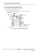
Page 6: ...bus Strobe mode connection example Set CPU_Config register 0x075h address BusMode bit to 0 and Bus8x16 bit to 0 16bit Strobe mode CPU S1R72V17 IOVDD CVDD Address 8 1 CA 8 1 XBEL CA 0 DATA 15 0 CD 15 0 XCS XCS XRD XRD XWRH XWRH XBEH XWRL XWRL XWR XDREQ XDREQ 1 XDACK XDACK 2 XINT XINT When DMA is not used 1 Open 2 Fixed at High or Low 1 65 V to 3 6 V Fig 2 1 16 bit bus Strobe mode connection example...

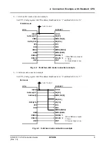
Page 7: ...Q XDREQ 1 XDACK XDACK 2 XINT XINT When DMA is not used 1 Open 2 Fixed at High or Low 1 65 V to 3 6 V Fig 2 2 16 bit bus BE mode connection example 3 8 bit bus mode connection example Set CPU_Config register 0x075h address BusMode bit to 0 and Bus8x16 bit to 1 8bit mode CPU S1R72V17 IOVDD CVDD Address 8 1 CA 8 1 Address 0 XBEL CA 0 CD 15 8 DATA 7 0 CD 7 0 XCS XCS XRD XRD XWRH XBEH XWR XWRL XWR XDRE...

Page 8: ...n the CPU_Config register 0x075h address CPU_Endian bit 1 Access to Word register The S1R72V17 connects the D 15 8 bus to the first byte of the Word register and the D 7 0 bus to the last byte of the Word register The example below illustrates the writing and reading of 0x1234h data to from the Word register Writing The data 12h in the CPU memory even number address is saved to the first byte of t...

Page 9: ... the Byte register odd number address register Writing The data F1h in the CPU memory even number address is saved to the S1R72V17 even number address register Reading The S1R72V17 even number address register data F1h is saved to the even number address in CPU memory CPU Data F1h Even number address F2h Odd number address Data in CPU memory Higher byte 15 8 Lower byte 7 0 F1h F2h CPU register D 1...

Page 10: ...ata C1h in the CPU memory even number address is sent from the USB bus as the first data Reading The first data received from the USB bus C1h is saved to the even number address in CPU memory CPU Data C1h Even number address C2h Odd number address Data in CPU memory Higher byte 15 8 Lower byte 7 0 C1h C2h CPU register D 15 8 D 7 0 CPU data bus D 15 0 bus connected unchanged S1R72V17 D 15 8 D 7 0 V...

Page 11: ...ng of 0x1234h data to from the Word register Writing The data 34h in the CPU memory even number address is saved to the last byte of the S1R72V17 Word register Reading The last byte data 34h of the S1R72V17 Word register is saved to the even number address in CPU memory CPU Data 34h Even number address 12h Odd number address Data in CPU memory Higher byte 15 8 Lower byte 7 0 12h 34h CPU register D...

Page 12: ...the Byte register odd number address register Writing The data F1h in the CPU memory even number address is saved to the S1R72V17 even number address register Reading The S1R72V17 even number address register data F1h is saved to the even number address in CPU memory CPU Data F1h Even number address F2h Odd number address Data in CPU memory Higher byte 15 8 Lower byte 7 0 F2h F1h CPU register D 15...

Page 13: ...a C1h in the CPU memory even number address is sent from the USB bus as the first data Reading The first data received from the USB bus C1h is saved to the even number address in CPU memory CPU Data C1h Even number address C2h Odd number address Data in CPU memory Higher byte 15 8 Lower byte 7 0 C2h C1h CPU register D 15 8 D 7 0 CPU data bus D 15 0 bus connected unchanged S1R72V17 D 15 8 D 7 0 V17...

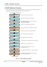
Page 14: ...071 address Write 0x00 to ChipReset register 0x011 address Write oscillation start time to WakeupTim_H L registers 0x014 address Write 0x40 to PM_Control register 0x012 address Read MainIntStat register 0x000 address to check that FinishedPM bit bit 0 is set to 1 Read write test to from AREA0StartAdrs_L H registers 0x080 address Read write test to from D_EPaIntEnb register 0x0C6 address and D_EPbI...

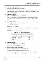
Page 15: ...us8x16 bits Little endian CPU 0x74h address Big endian CPU 0x75h address This register address is assigned to the 0x075h address Since the S1R72V17 operates in the default big endian state until this setting is changed the 0x074h address should be accessed to access a little endian CPU Table 4 1 CPU_Config register settings Bus mode CPU endian Setting Little Endian 0x04 16 bit Strobe mode Big Endi...

Page 16: ...to the ChipReset register 0x011 address Clearing the bit7 ResetMTM bit to 0 clears the USB Transceiver Macro reset and enables oscillation of the PLL contained in the S1R72V17 9 Oscillation start time setting Write the oscillation start time to the WakeupTim_H L registers 0x014 address With external clock source Write 0x0010 Note that the external clock source oscillation must have stabilized befo...

Page 17: ... to confirm that an interrupt occurs in the CPU Writing 1 to the MainIntStat register 0x000 address bit 0 FinishedPM bit clears this status Read the MainIntStat register 0x000 address bit 0 FinishedPM bit again to confirm that it has been cleared to 0 12 Synchronous register access test Word register Read write test to from the AREA0StartAdrs_L H registers 0x080 address These registers can be read...

Page 18: ... the S1R72V17 16 bit BE mode bus mode iMX21 MC9328MX21 S1R72V17 NVDD1 to 6 CVDD A 8 1 CA 8 1 D 15 0 CD 15 0 CS1 XCS OE PC_IOWR XRD EB3 DQM3 PC_IORD XBEL CA 0 EB2 DQM3 PC_REG XWRH XBEH RW PC_WE XWRL XWR CSPI1_RDY XDREQ LD16 XDACK LD17 XINT Typ 1 8V Fig 5 1 Connection example with iMX21 1 CPU IF power supply voltage In this connection example the CPU IF supply voltage is Typ 1 8 V iMX21 IO supply vo...

Page 19: ...shared pins are set as shown below in this connection example Table 5 1 iMX21 shared pin settings iMX21 pin name iMX21 pin function NVDD1 to NVDD6 NVDD1 to NVDD6 A 8 1 A 8 1 D 15 0 D 15 0 CS1 CS1 OE PC_IOWR OE EB3 DQM3 PC_IORD EB3 EB2 DQM2 PC_REG EB2 RW PC_WE RW CSPI1_RDY EXT_DMAREQ LD16 EXT_DMAGRANT LD17 PA23 GPIO used as XINT ...

Page 20: ... 14 13 12 11 10 9 8 7 6 5 4 3 2 1 0 EBC PSR CRE WRAPCSEN Setting descriptions Register Setting Description RWA 4 b0100 RW output assert timing 2HCLK SYNC 1 b0 Synchronous transfer mode disabled RWN 4 b0010 RW output negate timing 1HCLK WSC 6 b000111 Access cycle 8HCLK WWS 3 b000 Wait cycle for write 0HCLK OEA 4 b0100 OE output assert timing 2HCLK OEN 4 b0010 OE output negate timing 1HCLK WEA 4 b00...

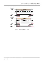
Page 21: ...orm Read cycle Bus cycle Read access HCLK bus clock A 8 1 O A0 CS1 O OE O Write cycle Bus cycle Write access HCLK bus clock A 8 1 O A0 CS1 O RW O EB3 2 O CSA 0HCLK CSN 0HCLK OEA 2HCLK OEN 1HCLK WSC 8HCLK CSA 0HCLK CSN 0HCLK RWA 2HCLK RWN 1HCLK WSC 8HCLK WEA 0HCLK WEN 0HCLK Fig 5 3 iMX21 bus cycle waveform ...

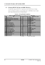
Page 22: ...S setup time 6 2 HCLK RWA OEA tcch XCS hold time 6 1 HCLK RWN OEN trcy Read cycle 80 8 HCLK WSC tras Read strobe assert time 40 5 HCLK WSC OEA OEN trng Read strobe negate time 25 3 HCLK OEA OEN trbd Read data output start time 1 trdf Read data confirmation time 35 5 HCLK WSC OEA OEN trdh Read data hold time 3 trbh Read data output delay time 9 twcy Write cycle 80 8 HCLK WSC twas Write strobe asser...

Page 23: ...Revision History Revision History Revision details Date Rev Page Type Details 06 06 2008 1 0 All New Newly created ...

Page 24: ...chai Hong Kong Phone 852 2585 4600 FAX 852 2827 4346 Telex 65542 EPSCO HX EPSON CHINA CO LTD SHENZHEN BRANCH 12 F Dawning Mansion Keji South 12th Road Hi Tech Park Shenzhen Phone 86 755 2699 3828 FAX 86 755 2699 3838 EPSON TAIWAN TECHNOLOGY TRADING LTD 14F No 7 Song Ren Road Taipei 110 Phone 886 2 8786 6688 FAX 886 2 8786 6660 EPSON SINGAPORE PTE LTD 1 HarbourFront Place 03 02 HarbourFront Tower O...

Reviews: