S1R72803F00A
EPSON
105
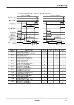
P_BCLK
P_A[23:0]
P_CE
X
P_WR
X
_X
P_D[15:0]
P_P30
(Wait input)
C
1
C
W
(Wait cycle)
C
W
(Wait cycle)
Cn (Last cycle)
Next is also wait cycle
Next is last cycle
t
AD
t
AD
t
WDH
t
WRD2
t
CE1
t
WRD1
t
WDD1
t
WTS
t
WTH
t
WTS
t
WTH
t
WTS
t
WRW
t
WTH
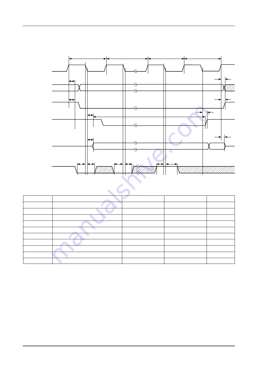
9.4.4.2 CPU Write Cycle
Symbol
Specification
Min.
Max.
Unit
t
AD
Address delay time
–
8
ns
t
CE1
P_CEx delay time (1)
–
8
ns
t
CE2
P_CEx delay time (2)
–
8
ns
t
WTS
Wait set-up time
29
–
ns
t
WTH
Wait hold time
0
–
ns
t
WRD1
Write signal delay time (1)
–
8
ns
t
WDD1
Write data delay time (1)
–
10
ns
t
WDH
Write data hold time
0
–
ns
t
WRD2
Write signal delay time (2)
–
8
ns
t
WRW
Write signal pulse width
t
CYC
(1+WC)–10
–
ns
*
t
CYC
=40ns when bus clock is 25MHz in X2 mode.
* WC: Wait cycle signal
Regarding the built-in CPU, refer to the S1C33208/204/202 Technical Manual and S1C33 Family ASIC Macro Manual.
In the built-in CPU core, however, a DMA controller or A/D converter are not integrated; this part is different from the
description on the DMA controller and A/D converter given in the Technical Manual and Macro Manual. Both low-
speed oscillation circuit (OSC1) and high-speed oscillation circuit (OSC4) are not available.

