S1R72803F00A
EPSON
17
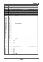
7.3 IEEE1394 HARDWARE SBP-2 CONTROL
The hardware SBP2 of this IC automatically executes a
PageTable fetch and data transfer according to the
Serial Bus Protocol 2 after receiving specifications of
its PageTable Size and Address. The control of the
SBP2 is performed by accessing the internal register.
Data transfer is controlled by the transmission and
reception of signals to and from the PHY-LINK interface
and the transmission/reception of a series of packets are
automatically executed by having access to the internal
SRAM area. The functions of this block are as follows.
This Block,
(1) Receives specifications of a Page Table Size, Page
Table Address, Speed Code, and Max Payload Size,
etc. to automatically execute a PageTable fetch and
data transfer according to the Serial Bus Protocol 2.
(2) Can transfer data the equivalent of max. 24-page
elements at one time. If no PageTable exists, you
can transfer data by directly specifying a data length
as a Page Table Size.
(3) Allows you to perform the pause, resume, or reset
during data transfer. Though the register value is
retained even after the reset, the state machine is
restored to the initial state. You can check transfer
condition through the register any time.
(4) Immediately enters the error pause when an error
arises during data transfer by which you can check
an error cause through the register. The resume
from the error pause will pick up the transaction
where the error arose.
(5) Allows you to transfer data if you specify the
omission of the PageTable fetch or Page Element
No. to start data.
7.5 BUILT-IN CPU
Regarding the built-in CPU, refer to the S1C33208/204/
202 TECHNICAL MANUAL (and S1C33 Family ASIC
Macro Manual).
In the built-in CPU core, however, a DMA controller
and A/D converter are not integrated; this part is different
from the description on the DMA controller and A/D
converter given in TECHNICAL MANUAL (and Macro
Manual). A low speed oscillation circuit (OSC1) is not
available.
7.4 IDE INTERFACE CONTROL
This IC contains a block to control the IDE interface. Its
functions are as follows.
This block,
(1) Accesses the IDE bus by having access to the
Program mode of the CPU.
The access to the data port of the CPU is available
only in PIO mode.
(2) Can monitor various kinds of signals of the IDE
interface.
(3) Controls the link-up of function blocks in accordance
with the control signals and operation end signal
from the DMA control circuit.
(4) Manages the condition of data transfer in DMA
mode of the IDE by the HDMARQ/XHDMACK
signal.
(5) Reads and writes the data of data bus DD15-0 of
IDE from and to the FIFO in the 1394LINKCORE
by the XHIOR/XHIOW signal.
If the FIFO becomes full or empty to disable data
transfer, this block suspends data transfer with
specified timing.


