background image

S1R72803F00A

18

EPSON

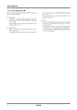
7.6  FLASH CONTROLLER

This IC is provided with a function to perform Erase and
Write to the Flash ROM.

(1) Chip Erase

According to a specified sequence, you can erase all
memory cells in the built-in Flash ROM to put them
in “1” status.
After erasing the chip, check that the data of all
memory cells is “1”.

(2) Sector Erase

This IC is ready for the Sector Erase in the unit of
512 words/sector.
According to a specified sequence, you can erase all

memory cells in the built-in Flash ROM to put them
in “1” status.
After erasing the chip, check that the data of all
memory cells is “1”.

(3) Write

Write is complete if you continue writing Write data
in the unit of word until writing of all sectors (512
words) finishes.
On completion of the Sector Write, compare all data
in the sectors with original data for confirmation.
You cannot change the data of the memory cell from
“0” to “1” by writing.

Summary of Contents for S1R75801F00A

Page 1: ...4 Controller S1R75801F00A Technical Manual S1R72803F00A EPSON Electronic Devices Website ELECTRONIC DEVICES MARKETING DIVISION First issue September 2001 Printed June 2003 in Japan H A 4 5mm Technical Manual IEEE1394 Controller S1R72803F00A http www epsondevice com ...

Page 2: ...ucts requiring high level reliability such as medical products Moreover no license to any intellectual property rights is granted by implication or otherwise and there is no representation or warranty that anything made in accordance with this material will be free from any patent or copyright infringement of a third party This material or portions thereof may contain technology or the subject rel...

Page 3: ...se the new product number when you place an order For further information please contact Epson sales representative Configuration of product number DEVICES S1 R 72803 F 00A1 00 Packing specification Specifications Shape F QFP Model number Model name R Exclusive use controller Peripheral Product classification S1 Semiconductors ...

Page 4: ...INTERFACE CONTROL 17 7 5 BUILT IN CPU 17 7 6 FLASH CONTROLLER 18 8 INTERNAL REGISTER 19 8 1 IEEE1394 LINK CONTROLLER REGISTER MAPPING 19 8 1 1 Register Table 19 8 1 2 Register Bit Table 22 8 1 3 Register Map 26 8 1 4 Detail Description of Register 42 8 2 FLASH ROM CONTROL REGISTER 88 9 ELECTRICAL CHARACTERISTICS 91 9 1 ABSOLUTE MAXIMUM RATINGS 91 9 2 RECOMMENDED OPERATING CONDITION 91 9 3 DC CHARA...

Page 5: ...ger by hardware Transaction Layer Integrates a part of transaction functions into hardware to prevent deterioration of actual data transmission rate due to the overhead of firmware assure a special area A header area is distinguished from a data area to simplify communications with a higher rank layer Furthermore it segments a data area to a stream area and ORB area Adopts a ring buffer to the rec...

Page 6: ...reset Built in RAM 8Kbytes for work Flash ROM Integration of a Flash ROM eliminated the necessity of a ROM to externally store programs Memory structure Memory size 512K 32K 16 bits Sector size 512 words sector Unit of erase Per chip or sector Unit of write Writing with words Erase write time Chip erase time 100ms Standard Sector erase time 20ms Standard Write time 15µs Standard Access time 90nsec...

Page 7: ...HDD 15 0 HDMARQ XHIOR XHIOW XHDMACK HIORDY HINTRQ XHPDIAG HDA 2 0 XCS 1 0 XHDASP XHRST EXCLK_EN OSC3 PLLS1 PLLS0 ICEMD DSIO X2SPD XNMI XREST TVEP C33 Internal Memory Block CORE PAD PERI PAD 3 2 BLOCK DIAGRAM DESCRIPTION C33 CORE Block The C33 CORE Block consists of the function block C33_CORE that includes the CPU BCU bus control unit ITC interrupt controller CLG clock generator and DBG debug unit...

Page 8: ...CSFREG XCE5 LPS P35 PD P34 CNA K64 K66 K67 P20 P21 P22 P23 xCSFLS XCE10 xWRL xRD xWait xRST xINT K65 SLEEP P33 U_AD 12 0 U_DT 7 0 xCSREG xCSBUF xWRL xRD xWait xRST xINT SLEEP U_AD 14 0 U_DT 15 0 xCSFREG xWRL U_AD 14 0 U_DT 15 0 Flash ROM 64KB FLASH Controller 1394LINK Core xCS xRD xRD HDD 15 0 HDA 2 0 XHCS 1 0 XHRST XHIOW BHEN MonxWait MonxInt XISO LINKON LPS LREQ CTL 1 0 D 7 0 SCLK XHIOR HDMARQ X...

Page 9: ...NA XISO BHEN CTL0 CTL1 D0 D1 D2 LV DD D3 D4 D5 D6 D7 PD LPS LINKON N C LV DD 92 91 90 89 88 87 86 85 84 83 82 81 80 79 78 77 76 75 74 73 72 71 70 69 68 67 66 65 64 63 62 61 60 59 58 57 56 55 54 53 52 51 50 49 48 47 VSS N C XHRST HDD7 HDD8 HDD6 HDD9 HDD5 HDD10 HVDD HDD4 HDD11 HDD3 HDD12 HDD2 HDD13 HDD1 VSS HDD14 HDD0 HDD15 HDMARQ XHIOW XHIOR HIORDY HVDD XHDMACK HINTRQ HDA1 XHPDIAG HDA0 HDA2 XHCS0 X...

Page 10: ...HEN 109 I Bus Holder Enable Signal H Single capacitor AC connection L DC connection CNA 111 I Cabele Not Active Schmitt Input Bus Holder PD 97 O Power Down Enable Drive Ability 6mA SCLK 113 I Clock Signal from PHY 49 576MHz Schmitt Input Bus Holder IDE Interface LVDD HDD15 72 B Hi Z MSB HDD14 74 B Hi Z HDD13 77 B Hi Z HDD12 79 B Hi Z HDD11 81 B Hi Z HDD10 84 B Hi Z HDD9 86 B Hi Z 5V Tolerant HDD8 ...

Page 11: ...tt Input XHRST 90 Otr Hi Z IDE Reset Signal Drive Ability 2mA Tristate C33 External Interface HVDD AD23 54 O MSB AD22 53 O AD21 52 O AD20 51 O AD19 50 O AD18 49 O AD17 44 O AD16 43 O AD15 42 O CPU Address Bus AD14 41 O AD13 40 O AD12 39 O AD11 38 O AD10 36 O AD9 35 O AD8 34 O AD7 33 O AD6 32 O AD5 31 O AD4 30 O AD3 28 O AD2 27 O AD1 26 O AD0 25 O LSB DT15 20 B Hi Z MSB DT14 19 B Hi Z DT13 18 B Hi ...

Page 12: ...Pull Up Resistor Integrated P21 136 B Generall I O Port 21 Pull Up Resistor Integrated P20 135 B Generall I O Port 20 Pull Up Resistor Integrated XCE10_EX 134 O Hi External Memory Area 10 Chip Enable XCE9 133 O Hi Area 9 Chip Enable XCE6 131 O Hi Area 6 Chip Enable EA10M2 164 I Area 10 Boot Mode Select 2 EA10M1 163 I Area 10 Boot Mode Select 1 Pull Up Resistor Integrated EA10M0 162 I Area 10 Boot ...

Page 13: ...Input Bus Holder TO7 122 O MSB TO6 123 O TO5 124 O TO4 125 O Test Output Pin Drive Ability 1mA TO3 126 O TO2 127 O TO1 128 O TO0 129 O LSB FLSTST 55 I Built in Flash Test Pin Pull Down Resistor Integrated RAMTST 156 I Built in SRAM Test Pin Pull Down Resistor Integrated MonxWait 132 O Internal Logic xWait Monitor Pin MonxInt 120 O Internal Logic xINT Monitor Pin Power Pin HVDD P HIGH Power 5V 5 21...

Page 14: ...Mirror of CPU integrated Peripheral Circuit Control Register Area 2 0x060000 Reserved Area 3 0x080000 Reserved Area 4 0x100000 IEEE1394LINK Transaction Controller x CSREG Area Control Register 0x100080 Reserved Area 5 0x200000 Flash ROM Control Register 0x200008 Reserved Area 6 0x300000 Reserved Area 7 0x400000 IEEE1394LINK Transaction Controller xCSBUF Area SRAM 8KB 0x402000 Reserved Area 8 0x600...

Page 15: ...xHeaderArea RxORBArea TxStreamArea and RxStreamArea monitor the used condition in each Area In the case of the Rx of 1394 the free space of the above two is monitored and the busy_A B X is controlled by hardware By controlling the above functions from the TRAN SBP2 Control Block a PageTable fetch and data transfer according to SBP 2 are executable by hardware 7 1 2 IEEE1394LINK Transaction Control...

Page 16: ...eserved 1 QuadReadReq tcode 0x4 DestinationID DestinationOffset 1 2 rcode 2 WriteResp tcode 0x2 DestinationID reserved 0 1 2 3 4 5 6 7 b 31 24 23 16 15 8 b 0 7 1 2 3 DestinationID Sbid speed tl rt pri ACK tcode MSB MSB LSB LSB PacketTypeSpecInfo PacketTypeSpecQuadletData reserved 1 QuadWriteReq tcode 0x0 DestinationID DestinationOffset QuadletData 1 2 3 2 QuadReadResp tcode 0x6 DestinationID reser...

Page 17: ...nt Description speed 3 Speed Code 3 b000 S100 3 b001 S200 3 b010 S400 All Other Value Reserved Sbid 1 Souce Bus ID 0 3FFh 1 Source ID 0 1 2 3 4 5 6 7 b 31 24 23 16 15 8 b 0 7 1 2 DestinationID DataLength speed tl rt pri ACK tcode MSB MSB LSB LSB PacketTypeSpecInfo DataPointer reserved ExtendedTcode 1 BlockWriteReq LockReq tcode 0x1 tcode 0x9 DestinationID DestinationOffset 1 2 rcode 2 BlockReadRes...

Page 18: ...eserved 1 QuadReadReq tcode 0x4 SourceID DestinationOffset 2 3 rcode 2 WriteResp tcode 0x2 SourceID reserved 0 1 2 3 4 5 6 7 b 31 24 23 16 15 8 b 0 7 DestinationID SourceID speed tl BT 0 BC 0 AS rt ACK pri tcode MSB LSB PacketTypeSpecInfo PacketTypeSpecQuadData reserved 2 3 4 MSB LSB 1 QuadWriteReq tcode 0x0 SourceID DestinationOffset QuadletData 2 3 4 2 QuadReadResp tcode 0x6 SourceID reserved Qu...

Page 19: ...ataLength speed tl BT 0 BC 0 AS rt ACK pri tcode MSB MSB LSB LSB PacketTypeSpecInfo DataPointer ExtendedTcode reserved 1 BlockWriteReq LockReq tcode 0x1 tcode 0x9 SourceID DestinationOffset 2 3 rcode 2 BlockReadResp LockResp tcode 0x7 tcode 0xB SourceID reserved 0 1 2 3 4 5 6 7 b 31 24 23 16 15 8 b 0 7 0 x 0 BT 0 1 0 AS ACK reserved tcode 0xE PhyPacket reserved reserved 0 1 2 3 4 5 6 7 b 31 24 23 ...

Page 20: ... Speed Code Note 1 AS 1 AreaStatus bit 1 StreamArea 0 ORBArea BT 1 Bit which toggles during the BusReset period SI 1 Whether the received packet is a Self ID packet BC 1 Whether the received packet is a Broadcast packet HC 1 Presence absence of the Header CRC error 1 Packet disabled ACK 4 Transmitted AckCode Note 2 PSTS 4 AckCode which was scheduled to be transmitted Note 2 Note 1 Refer to the Tra...

Page 21: ... an error arises during data transfer by which you can check an error cause through the register The resume from the error pause will pick up the transaction where the error arose 5 Allows you to transfer data if you specify the omission of the PageTable fetch or Page Element No to start data 7 5 BUILT IN CPU Regarding the built in CPU refer to the S1C33208 204 202 TECHNICAL MANUAL and S1C33 Famil...

Page 22: ...is ready for the Sector Erase in the unit of 512 words sector According to a specified sequence you can erase all memory cells in the built in Flash ROM to put them in 1 status After erasing the chip check that the data of all memory cells is 1 3 Write Write is complete if you continue writing Write data in the unit of word until writing of all sectors 512 words finishes On completion of the Secto...

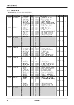
Page 23: ...rdware Revision Register 0x12 Reserved 0x13 Reserved 0x14 Reserved 0x15 Reserved 0x16 Reserved 0x17 Reserved 0x18 LinkCtl_H R W LINK Core Control Register Higher Rank 0x19 LinkCtl_L R W LINK Core Control Register Lower Rank 0x1A LinkStat R LINK Core Status Read Register 0x1B PriReqCnt R Priority Request Count Register 0x1C RetryLimit_H R W Dual Retry Time Set Register Higher Rank 0x1D RetryLimit_L...

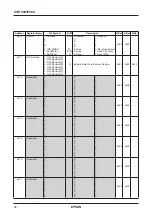
Page 24: ...ister Lower Rank 0x44 LinkRxStreamPtr_H R W Receive Stream Data LINK Pointer Register Higher Rank 0x45 LinkRxStreamPtr_L R W Receive Stream Data LINK Pointer Register Lower Rank 0x46 LinkTxStreamPtr_H R Receive Stream Data LINK Pointer Register Higher Rank 0x47 LinkTxStreamPtr_L R Receive Stream Data LINK Pointer Register Lower Rank 0x48 UsedRxHdrPtr_H R W Used Receive Header Pointer Register High...

Page 25: ... Register Lower Rank 0x6C IDE_CRC0 R CRC Read Register Higher Rank 0x6D IDE_CRC1 R CRC Read Register Lower Rank 0x6E Reserved 0x6F Reserved 0x70 IDE_CS00 R W IDE Command Block Register 0x71 IDE_CS01 R W IDE Command Block Register 0x72 IDE_CS02 R W IDE Command Block Register 0x73 IDE_CS03 R W IDE Command Block Register 0x74 IDE_CS04 R W IDE Command Block Register 0x75 IDE_CS05 R W IDE Command Block...

Page 26: ... EnDupliCh EnIsoArbFaild EnCycTooLon EnCycOverFlw EnCycEvent EnCycLost EnCycArbFail 0x0E PhyIntEnb EnSubGap EnArbGap EnPhy_int EnPhyWrDone EnPhyRdDone 0x0F Reserved 0x10 ChipCtl Suspend IDE_MdlRst SendTardy SoftReset 0x11 HW_Revision HW_Revision 7 0 0x12 ApetusTestOutPut_H 0x13 ApetusTestOutPut_L 0x14 LCTestIndex Chip Test Register 0x15 LCTestWindow 0x16 SBP2TestIndex 0x17 SBP2TestWindow 0x18 Link...

Page 27: ..._L LinkRxStreamPtr 7 2 0x46 LinkTxStreamPtr_H LinkTxStreamPtr 12 8 0x47 LinkTxStreamPtr_L LinkTxStreamPtr 7 2 0x48 UsedRxHdrPtr_H UsedRxHdrPtr 12 0x49 UsedRxHdrPtr_L UsedRxHdrPtr 7 5 0x4A UsedRxORBPtr_H UsedRxORBPtr 12 8 0x4B UsedRxORBPtr_L UsedRxORBPtr 7 2 0x4C IDE_RxStreamPtr_H IDE_RxStreamPtr 12 8 0x4D IDE_RxStreamPtr_L IDE_RxStreamPtr 7 2 0x4E IDE_TxStreamPtr_H IDE_TxStreamPtr 12 8 0x4F IDE_Tx...

Page 28: ...ence W Not Used 0x79 IDE_CS11 Control Block Register R Data Bus Hi Impedence W Not Used 0x7A IDE_CS12 Control Block Register R Data Bus Hi Impedence W Not Used 0x7B IDE_CS13 Control Block Register R Data Bus Hi Impedence W Not Used 0x7C IDE_CS14 Control Block Register R Data Bus Hi Impedence W Not Used 0x7D IDE_CS15 Control Block Register R Data Bus Hi Impedence W Not Used 0x7E IDE_CS16 Control Bl...

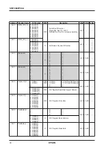
Page 29: ...edCode 2 0 MaxPayload MaxPayload 3 0 0x03 DestinationID_H MSB DestinationID_L Destination_ID Value LSB 0x04 SplitTime_H Second 2 0 Cycle Count 12 8 SplitTime_L Cycle Count 7 0 0x05 Reserved Reserved 0x0F Reserved Memory Map Area Index Window Register AreaIndex AreaWindow_H L bit7 bit6 bit5 bit4 bit3 bit2 bit1 bit0 0x00 RxORBAreaStart_H MSB RxORBAreaStart 12 8 RxORBAreaStart_L RxORBAreaStart 7 2 LS...

Page 30: ...ld R W 0 None 1 Rx DMA Failed 0x00 0x00 3 TxAsyFaild R W 0 None 1 Async Tx Failed 2 TxIsoFaild R W 0 None 1 ISO Tx Failed 1 TxAsyBRAbort R W 0 None 1 Async Tx BusReset Abort 0 TxAsyMiss R W 0 None 1 AsyncTxAckCodeMissing 0x04 LinkIntStat1 7 0 1 6 0 1 5 0 1 4 1 0x00 0x00 3 RxOnTardy R W 0 None 1 Ack_tardy Sent 2 RxHcrcErr R W 0 None 1 Rx Packet Header CRC Err 1 RxUnkTcode R W 0 None 1 Rx Packet Tco...

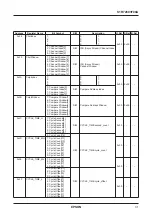
Page 31: ... 1 Enable 5 EnTxAsyBCSent R W 0 Disable 1 Enable 4 EnRxDmaFaild R W 0 Disable 1 Enable 0x00 0x00 3 EnTxAsyFaild R W 0 Disable 1 Enable 2 EnTxIsoFaild R W 0 Disable 1 Enable 1 EnTxAsyBRAbort R W 0 Disable 1 Enable 0 EnTxAsyMiss R W 0 Disable 1 Enable 0x0C LinkIntEnb1 7 0 1 6 0 1 5 0 1 4 0 1 0x00 0x00 3 EnRxOnTardy R W 0 Disable 1 Enable 2 EnRxHcrcErr R W 0 Disable 1 Enable 1 EnRxUnkTcode R W 0 Disa...

Page 32: ...Revision 4 R Indicate Hard Ware Revison Number 0x03 0x03 0x03 3 HW_Revision 3 2 HW_Revision 2 1 HW_Revision 1 0 HW_Revision 0 0x12 Reserved 7 0 1 6 0 1 5 0 1 4 0 1 0x00 0x00 3 0 1 2 0 1 1 0 1 0 0 1 0x13 Reserved 7 0 1 6 0 1 5 0 1 4 0 1 0x00 0x00 3 0 1 2 0 1 1 0 1 0 0 1 0x14 Reserved 7 0 1 6 0 1 5 0 1 4 0 1 0x00 0x00 3 0 1 2 0 1 1 0 1 0 0 1 0x15 Reserved 7 0 1 6 0 1 5 0 1 4 0 1 0x00 0x00 3 0 1 2 0 ...

Page 33: ...y Enable 0 0x1A LinkStat 7 0 1 6 0 1 5 0 1 4 0 1 0x00 3 0 1 2 ID_Valid R 0 PhyID Invalid 1 PhyID Valid 1 Root R 0 Self Node Not Root 1 Self Node Root 0 CablPwSts R 0 Cable Power Status NG 1 Cable Power Status OK 0x1B PriReqCnt 7 0 1 6 0 1 5 PriReq 5 4 PriReq 4 0x00 0x00 0x00 3 PriReq 3 R W Maximum Number of certain Priority Arb Request 2 PriReq 2 1 PriReq 1 0 PriReq 0 0x1C RetryLimit_H 7 SecLimit ...

Page 34: ... 0 1 1 0 1 0 0 1 0x23 Reserved 7 0 1 6 0 1 5 0 1 4 0 1 0x00 0x00 3 0 1 2 0 1 1 0 1 0 0 1 0x24 PhyAccCtl_H 7 RdReq R W 0 Normal 1 PHY Reg Rd Request 6 WrReq R W 0 Normal 1 PHY Reg Wr Request 5 0 1 4 0 1 0x00 0x00 3 ReqAdd 3 2 ReqAdd 2 R W PHY Register Read Write Request Address 1 ReqAdd 1 0 ReqAdd 0 0x25 PhyAccCtl_L 7 WrDat 7 6 WrDAt 6 5 WrDat 5 4 WrDat 4 R W PHY Register Write Data 0x00 0x00 3 WrD...

Page 35: ... Compare Window 5 4 Compare Window 4 R W Compare Address Window 0x00 0x00 3 Compare Window 3 2 Compare Window 2 1 Compare Window 1 0 Compare Window 0 0x2C CYCLE_TIME_H 7 Cycle Second 6 6 Cycle Second 5 5 Cycle Second 4 4 Cycle Second 3 R W CYCLE_TIME second_count 0x00 3 Cycle Second 2 2 Cycle Second 1 1 Cycle Second 0 0 Cycle Count 12 0x2D CYCLE_TIME_MH 7 Cycle Count 11 6 Cycle Count 10 5 Cycle Co...

Page 36: ...00 0x00 3 NotQuad R W 0 None 1 NotQuad 2 RxNotRespCmp R W 0 None 1 RxNotRespCmp 1 RxBroadCast R W 0 None 1 RxBroadCast 0 RxAckDataErr R W 0 None 1 RxAckDataErr 0x33 HwSBP2Index 7 0 1 6 0 1 5 0 1 4 0 1 0x00 0x00 3 HwSBP2 Index 3 2 HwSBP2 Index 2 R W HwSBP2 Index 1 HwSBP2 Index 1 0 HwSBP2 Index 0 0x34 HwSBP2Window_H 7 HwSBP2 Window 15 6 HwSBP2 Window 14 5 HwSBP2 Window 13 4 HwSBP2 Window 12 0x00 0x0...

Page 37: ...dress 46 5 PtAdress 45 4 PtAdress 44 0x00 0x00 3 PtAdress 43 2 PtAdress 42 1 PtAdress 41 0 PtAdress 40 0x3B PageTableAdrs1 7 PtAdress 39 6 PtAdress 38 5 PtAdress 37 4 PtAdress 36 0x00 0x00 3 PtAdress 35 2 PtAdress 34 1 PtAdress 33 0 PtAdress 32 0x3C PageTableAdrs2 7 PtAdress 31 6 PtAdress 30 5 PtAdress 29 4 PtAdress 28 0x00 0x00 3 PtAdress 27 2 PtAdress 26 1 PtAdress 25 0 PtAdress 24 R W Write Set...

Page 38: ...t Received Packet ORB Data Area Pointer 6 POP 6 5 POP 5 4 POP 4 0x00 0x00 3 POP 3 2 POP 2 1 Write is ignore 0 Read is always zero 0x44 LinkRxStreamPtr_H 7 Write is ignore 6 Read is always zero 5 4 PSP 12 0x00 0x00 3 PSP 11 2 PSP 10 1 PSP 9 0 PSP 8 0x45 LinkRxStreamPtr_L 7 PSP 7 R W Current Received Packet Stream Data Area Pointer 6 PSP 6 5 PSP 5 4 PSP 4 0x00 0x00 3 PSP 3 2 PSP 2 1 Write is ignore ...

Page 39: ...t ORB Data Area Used Pointer 6 UOP 6 5 UOP 5 4 UOP 4 0x00 0x00 3 UOP 3 2 UOP 2 1 Write is ignore 0 Read is always zero 0x4C IDE_RxStreamPtr_H 7 Write is ignore 6 Read is always zero 5 4 IRSP 12 0x00 0x00 3 IRSP 11 2 IRSP 10 1 IRSP 9 0 IRSP 8 0x4D IDE_RxStreamPtr_L 7 IRSP 7 R W Received Packet Stream Data Area IDE Pointer 6 IRSP 6 5 IRSP 5 4 IRSP 4 0x00 0x00 3 IRSP 3 2 IRSP 2 1 Write is ignore 0 Re...

Page 40: ...0x00 0x00 3 AsyFIFOEpty R 0 AsyFIFO Empty 1 Non Empty 2 AsyFIFOClr W 0 Normal 1 AsyFIFO Clear 1 AsyTxMon R 0 Async Tx Stop 1 Async Tx Run 0 AsyStart W 0 normal 1 Async Start 0x53 IsoDmaCtl 7 IsoChnlSel R W 0 IsoTxPktHdr0 1 IsoTxPktHdr1 6 0 1 5 0 1 4 SelTxPtr R W 0 Async Tx Pointer Select 1 ISO Tx Pointer Select 0x00 0x00 3 IsoFIFOEpty R 0 IsoFIFO Empty 1 Non Empty 2 IsoFIFOClr W 0 Normal 1 IsoFIFO...

Page 41: ...usRstORBPtr 9 0 BusRstORBPtr 8 0x5B BRstORBPtr_L 7 BusRstORBPtr 7 R Bus Reset ORB Data Area Pointer 6 BusRstORBPtr 6 This register indicates Address in Rx ORB Data Area 5 BusRstORBPtr 5 when BusRest detected 4 BusRstORBPtr 4 0x00 0x00 3 BusRstORBPtr 3 2 BusRstORBPtr 2 1 Write is ignore 0 Read is always zero 0x5C Reserved 7 0 1 6 0 1 5 0 1 4 0 1 0x00 0x00 3 0 1 2 0 1 1 0 1 0 0 1 0x5D Reserved 7 0 1...

Page 42: ...3 6 Assert Pulse 2 R W IDE Transfer Mode Strobe Signal Assert Pulse 5 Assert Pulse 1 Width Minimum Value 4 Assert Pulse 0 0x00 0x00 3 Negate Pulse 3 2 Negate Pulse 2 R W IDE Transfer Mode Strobe Signal Negate Pulse 1 Negate Pulse 1 Width Minimum Value 0 Negate Pulse 0 0x64 IDE_UltraDmaCyc 7 0 1 6 0 1 5 0 1 4 0 1 3 Cycle Time 3 0x00 0x00 2 Cycle Time 2 R W IDE Ultra DMA Transfer Mode Strobe Signal ...

Page 43: ...otal Transfer Byte Count 0x6A IDE_ByteCount2 7 ByteCount 15 6 ByteCount 14 5 ByteCount 13 4 ByteCount 12 0x00 0x00 3 ByteCount 11 2 ByteCount 10 1 ByteCount 9 0 ByteCount 8 0x6B IDE_ByteCount3 7 ByteCount 7 6 ByteCount 6 5 ByteCount 5 4 ByteCount 4 0x00 0x00 3 ByteCount 3 2 ByteCount 2 1 ByteCount 1 0 ByteCount 0 0x6C IDE_CRC0 7 CRC 15 6 CRC 14 5 CRC 13 4 CRC 12 0x00 0x00 3 CRC 11 2 CRC 10 1 CRC 9...

Page 44: ...ock Register 5 4 R W Sector Number Register or 0x00 0x00 3 Logical Block Address LBA bit 0 7 2 1 0 0x74 IDE_CS04 7 6 Command Block Register 5 4 R W Cylinder Low Register or 0x00 0x00 3 Logical Block Address LBA bit 8 15 2 1 0 0x75 IDE_CS05 7 6 Command Block Register 5 4 R W Cylinder High Register or 0x00 0x00 3 Logical Block Address LBA bit 16 23 2 1 0 0x76 IDE_CS06 7 6 Command Block Register 5 4 ...

Page 45: ...Impedance 0x00 0x00 3 Write Not Used 2 1 0 0x7B IDE_CS13 7 6 Control Block Register 5 4 R W Read Data Bus Hi Impedance 0x00 0x00 3 Write Not Used 2 1 0 0x7C IDE_CS14 7 6 Control Block Register 5 4 R W Read Data Bus Hi Impedance 0x00 0x00 3 Write Not Used 2 1 0 0x7D IDE_CS15 7 6 Control Block Register 5 4 R W Read Data Bus Hi Impedance 0x00 0x00 3 Write Not Used 2 1 0 0x7E IDE_CS16 7 6 Control Bloc...

Page 46: ...p RxDmaCmp TxAsyCmp HwSBP2Cmp IDE_DmaCmp IDE_INTRQ and BusReset other than above is an interrupt source this register clears the bit by writing the read value Note The bits of this register control the XInt of output pin Writing to this register negates the XInt once even if the interrupt factor remains asserting the XInt after a certain period Ready for a timer or edge interrupt Bit7 Sub Interrup...

Page 47: ...IntStat Register exists this bit becomes 1 Bit4 BusReset in process HwSBP2 When a BusReset occurs in the HwSBP2 processing this bit becomes 1 Bit3 LINK Core Interrupt Status1 When an interrupt factor from the LINK core indicated on the LinkIntStat1 Register exists this bit becomes 1 Bit2 LINK Core Interrupt Status0 When an interrupt factor from the LINK core indicated on the LinkIntStat0 Register ...

Page 48: ...t Retry Go When an auto retry is performed after transmitting an Async packet and receiving an Ack_busy this bit becomes 1 Bit5 Transmit Async Broadcast Packet Sent After a transmission of a Broadcast packet of Async or a PHY packet finishes this bit becomes 1 Bit4 Receive Packet LINK DMA Failed When a received packet cannot be written to the buffer due to the following reasons this bit becomes 1 ...

Page 49: ...eturned to the party of the other end and this bit becomes 1 Bit2 Receive Packet Header CRC Error When an error exists in the header CRC of a received packet this bit becomes 1 Bit1 Receive Packet Tcode Unknown When the Tcode in a received packet is invalid this bit becomes 1 Bit0 transmit Retry Exceeded If a transmit retry fails since the set value of the MaxRetry Register is exceeded when the Re...

Page 50: ...ansmitted this bit becomes 1 Bit4 ISO Arbitration Failed When a Cycle_START packet is received but a SubAction Gap cannot be detected even after the ISOCHRONOUS_CYCLE_TIME has passed this bit becomes 1 Bit3 Cycle Timer Over Flow When the CYCLE_TIMER overflows this bit becomes 1 Bit2 Local Cycle Event Occurred When an local cycle event occurs this bit becomes 1 Bit1 Cycle Start Packet Lost When the...

Page 51: ...ter receiving the interrupt signal to locate an interrupt source By writing the read value again it clears these bits Bit 7 Sub Action Gap Detected When a Transmit Action Gap is detected in the PHY status of the PHY LINK interface this bit becomes 1 Bit6 Arbitration Reset Gap Detected When an Arbitration Reset Gap is detected in the PHY status of the PHY LINK interface this bit becomes 1 Bit5 Rese...

Page 52: ...ble 1 Enable 5 EnHwSBP2Err R W 0 Disable 1 Enable 4 EnHwSBP2BRst R W 0 Disable 1 Enable 0x00 0x00 3 EnLinkIntStat1 R W 0 Disable 1 Enable 2 EnLinkIntStat0 R W 0 Disable 1 Enable 1 EnPhyIntStat R W 0 Disable 1 Enable 0 EnDmaIntStat R W 0 Disable 1 Enable Address Register Name Bit Symbol R W Description H Rst S Rst B Rst 0x0A Reserved 7 0 1 6 0 1 5 0 1 4 0 1 0x00 0x00 3 0 1 2 0 1 1 0 1 0 0 1 Main In...

Page 53: ... W 0 Disable 1 Enable 2 EnRxHcrcErr R W 0 Disable 1 Enable 1 EnRxUnkTcode R W 0 Disable 1 Enable 0 EnTxRtyExced R W 0 Disable 1 Enable LINK Core Interrupt Enable Flag Register 1 This register enables disables an interrupt factor of the LINKIntStat1 Register Setting the corresponding bit to 1 enables an interrupt to the CPU Address Register Name Bit Symbol R W Description H Rst S Rst B Rst 0x0D Lin...

Page 54: ...IDE_MdlRst Setting this bit to 1 resets IDE related registers 0x60 0x7F to restore them to the initial state Bit1 Send Ack_tardy Enable Makes setting to return an Ack_tardy as a Ack code when receiving an Async packet 0 Usual Ack code 1 ack_tardy Bit0 Soft Reset Setting this bit to 1 initializes the interiors of the circuit After initializing it it is restored to 0 Address Register Name Bit Symbol...

Page 55: ...trol Register Higher Rank This register controls the functions of the LINK core Bit7 Pass Self ID Packet Setting this bit to 1 captures a Self ID packet received by the LINK core into the buffer Bit6 Pass PHY Packet When requesting the PHY Register for a register write this bit is set to 1 After the execution this bit is cleared Bit5 Pass BusReset Packet Setting this bit to 1 captures a BusReset p...

Page 56: ... is ignored Bit0 Single Phase Retry Enable Controls whether the Single Phase retry protocol is enabled When this bit is 1 a retry processing is done until the number set on the Retry Limit Register is exceeded When it is 0 a retry processing is disabled When the value of the MaxRetry Register is 0 a retry processing is ignored Address Register Name Bit Symbol R W Description H Rst S Rst B Rst 0x19...

Page 57: ...C Bit7 5 Second_Limit 2 0 Set a Dual Phase Retry Time Unit second 0x1C 0x1D Cycle Limit 12 0 Sets a retry time at Cycle Limit 12 0 Unit 125µs Address Register Name Bit Symbol R W Description H Rst S Rst B Rst 0x1B PriReqCnt 7 0 1 6 0 1 5 PriReq 5 4 PriReq 4 0x00 0x00 0x00 3 PriReq 3 R W Maximum Number of certain Priority Arb Request 2 PriReq 2 1 PriReq 1 0 PriReq 0 Priority Request Count Register ...

Page 58: ...hase Retry is ignored Bit7 4 Reserved Bit3 0 Single Retry Limit 3 0 Sets the number of retries in the Single Phase at maxRtry 3 0 IRM Status Register This IRM Status Register controls detection of the Isochronous Resource Manager Bit7 No IRM Sets whether an Isochronous Resource Manager exists on the serial bus 1 indicates the IRM node does not exist and 0 indicates the IRM node exists Bit6 WonIRM ...

Page 59: ...at the time of BusReset and is automatically stored on completion of the Self ID processing 0x20 0x21 Bit7 6 Bus ID These bits are areas to store the Bus_ID value of the serial bus 0x21 Bit5 0 PHY ID Indicates the Physical ID of a node established by the PHY in the Self ID phase Address Register Name Bit Symbol R W Description H Rst S Rst B Rst 0x24 PhyAccCtl_H 7 RdReq R W 0 Normal 1 PHY Reg Rd Re...

Page 60: ...Dat 1 0 RdDat 0 PHY Register Access Control Register Lower Rank Bit7 0 PHY Write Data Set data to write to the PHY Register PHY Register Read Status Register Higher Rank Bit7 Reserved Bit6 Reserved Bit5 Reserved Bit4 Reserved Bit3 0 PHY Read Address Indicate a register address indicated in the PHY status PHY Register Read Status Register Lower Rank Bit7 0 PHY Read Data Indicate register data indic...

Page 61: ...hannel This is a register to set an ISO channel number to be received by this IC ChnlIndex ChnlWindow bit7 bit6 bit5 bit4 bit3 bit2 bit1 bit0 0x00 ChannelAvailableH0 ch01 ch02 ch03 ch04 ch05 ch06 ch07 0x01 ChannelAvailableH1 ch08 ch09 ch10 ch11 ch12 ch13 ch14 ch15 0x02 ChannelAvailableH2 ch16 ch17 ch18 ch19 ch20 ch21 ch22 ch23 0x03 ChannelAvailableH3 ch24 ch25 ch26 ch27 ch28 ch29 ch30 ch31 0x04 Ch...

Page 62: ...received the received data of payload is received by the RxStreamArea 0x2A Compare Index This is a register to set an index number to select a channel 0x2B Compare Window This is a register to view a window specified by the Compare Index Compare Destination Offset Address When the BlkWrAreaSet bit is 1 and a BlockWriteRequest packet having an Destination_Offset address same as a value set to this ...

Page 63: ...very time the Cycle Offset reached 3072 When the Cycle Count reaches 8000 it is restored to 0 CYCLE_TIME cycle offset When the self node is a CYCLE TIMER and the DisCycTimer 0 it is incremented in a cycle of 24 576MHz When the Cycle Offset reaches 3072 it is restored to 0 and then the Cycle Count is incremented Address Register Name Bit Symbol R W Description H Rst S Rst B Rst 0x2C CYCLE_TIME_H 7 ...

Page 64: ...Stream 0 FromPt Set Starts with the PageTable Processing FromStream 1 FromStream Set Starts with the Stream processing Bit4 LastPT This bit indicates the 0x32 bit 3 NotQuad status and specifies whether to generate an interrupt if SegmentLength of the last PageTableElement on PageTable is not the Quad unit during the HwSBP2 process LastPT 0 None Set The NotQuad status is indicated for the last Page...

Page 65: ...f SegmentLength of PageTableElement is not the Quad unit during the HwSBP2 process NotQuadEnable 0 Disable Set A NotQuad interrupt is not generated NotQuadEnable 1 Enable Set A NotQuad interrupt is generated Note that this bit does not indicate the status of HwSBP2 Bit4 Wait Payload Ready WaitPLReady 0 Not Ready Payload Domain Not Ready WaitPLReady 1 Ready Payload Domain Ready When the IDE interfa...

Page 66: ...l 1 Though a transmission was completed a response other than ack_pending was given to a BlkRdReq and a response other than ack_completed was given to a BlkWrReq Bit5 Tx Ack Miss TxAsyMiss 1 Though a transmission was completed no Ack was returned Bit4 BRAbort When the HwSBP2Ctl HwSBP2Start bit is set to 1 or HWSBP2Ctl Resume bit is set to 1 during the BusReset period this bit becomes 1 Bit3 NotQua...

Page 67: ...ow 11 2 HwSBP2 Window 10 1 HwSBP2 Window 9 0 HwSBP2 Window 8 R W HwSBP2 Window 0x35 HwSBP2Window_L 7 HwSBP2 Window 7 6 HwSBP2 Window 6 5 HwSBP2 Window 5 4 HwSBP2 Window 4 0x00 0x00 3 HwSBP2 Window 3 2 HwSBP2 Window 2 1 HwSBP2 Window 1 0 HwSBP2 Window 0 Hardware SBP2 Index Window Register This register functions as an Index Register and Window Register to set a register to use for the HwSBP2 proces...

Page 68: ...e HwSBP2Ctl PtPresent 0 set a value equal to or less than 0x02 If you read it the page element number currently in process is indicated PgElementRemain Indicates the number of remaining data bytes of the page element currently being processed by the HwSBP2 This register is read only SpeedCode Sets the speed code of 1394 bus to be used for data transfer by the HwSBP2 SpeedCode 0 100Mbps SpeedCode 1...

Page 69: ...t Register The Write and Read of this register have different meanings depending on whether a PageTable is present setting of HwSBP2Ctl PtNotPresent bit When a PageTable is present Write Set a PageTable size in byte The number of pages x 8 bytes Read Indicates the remaining PageTable size When a PageTable is not present Write Set a data length Read Indicates a new PageTable size based on the writt...

Page 70: ...dicate NextPageTable Offset Address 6 PtAdress 22 5 PtAdress 21 4 PtAdress 20 0x00 0x00 3 PtAdress 19 2 PtAdress 18 1 PtAdress 17 0 PtAdress 16 0x3E PageTableAdrs4 7 PtAdress 15 6 PtAdress 14 5 PtAdress 13 4 PtAdress 12 0x00 0x00 3 PtAdress 11 2 PtAdress 10 1 PtAdress 9 0 PtAdress 8 0x3F PageTableAdrs5 7 PtAdress 7 6 PtAdress 6 5 PtAdress 5 4 PtAdress 4 0x00 0x00 3 PtAdress 3 2 PtAdress 2 1 PtAdre...

Page 71: ...gher order bytes holds the lower order bytes Read the higher order bytes first then the lower order bytes Receive ORB Data LINK Pointer Register This Receive ORB Data LINK Pointer Register indicates the starting address of the latest receive ORB data in the RxORBdataArea Since the buffer pointer is in Quadlet unit the lower order 2 bits are always 0 Also since the buffer size is 2 Kbytes the highe...

Page 72: ...zero Receive Stream Data LINK Pointer Register This Receive Stream Data LINK Pointer Register indicates the starting address of the latest received stream data in the RxStreamdataArea Since the buffer pointer is in Quadlet unit the lower order 2 bits are always 0 Also since the buffer size is 2 Kbytes the higher order 3 bits are always 0 Reading the higher order bytes holds the lower order bytes R...

Page 73: ... Area Used Pointer 0 URHP 8 0x49 UsedRxHdrPtr_L 7 URHP 7 6 URHP 6 5 URHP 5 4 0x00 0x00 3 Write is ignore 2 Read is always zero 1 0 Used Receive Header Pointer Register This Used Receive Header Pointer Register indicates the starting address of used header of a receive packet in the RxHdrArea Since the buffer pointer is in 8Quadlet unit the lower order 5 bits are always 0 Also since the buffer size...

Page 74: ...ter Register This Receive Stream Data IDE Pointer Register indicates the starting address of received stream data in the RxSTreamArea that is to be transmitted to the IDE side but not yet transmitted Since the buffer pointer is in Quadlet unit the lower order 2 bits are always 0 Also since the buffer size is 2 Kbytes the higher order 3 bits are always 0 Reading the higher order bytes holds the low...

Page 75: ...tes zero bit7 Tx Stream Clear Writing 1 to this bit changes the values of LINKTxStreamPtr and IDE_TxStreamPtr to ones set by the TxStreamAreaStart Register bit6 Rx Stream Clear Writing 1 to this bit changes the values of LINKRxStreamPtr and IDE_RxStreamPtr to ones set by the RxStreamAreaStart Register bit5 Rx ORB Clear Writing 1 to this bit changes the values of LINKRxORBPtr and IDE_RxORBPtr to on...

Page 76: ...Received Header Remain When an unused packet header exists in the header area of a receive packet this bit becomes 1 When the firmware rewrites the UsedRxHdrPtr to one same as LINKRxHdrPtr or when you write 1 to the BufControl RxHdrCtr bit this bit becomes 0 Bit2 Received ORB Data Full When the ORB buffer area of receive packet data is full of received data this bit becomes 1 The firmware must tur...

Page 77: ...t4 Block Write Request Packet Data Area Select Can divide the store area of the Block Write Request packet data between the RxORBArea and RxStreamArea o RxORBArea 1 RxStreamArea Bit3 Async FIFO Empty When the DMA FIFO for Async is empty this bit becomes 0 When it is not empty it is 1 This bit is read only and writing to this bit is ignored Bit2 Async FIFO Clear Clears the DMA FIFO for Async Writin...

Page 78: ...Pointer Can switch the address pointed by the PostTxDataPtr of a transmit packet to one for Async or ISO The PostTxData Ptr indicates a pointer of current transmit address 0 indicates it is for Async and 1 indicates it is for ISO Bit3 ISO FIFO Empty When the DMA FIFO for ISO is empty this bit becomes 0 When it is not empty it is 1 This bit is read only and writing to this bit is ignored Bit2 ISO F...

Page 79: ...bit clears the FIFO After clearing it this bit is automatically restored to 0 Bit1 Reception Monitor Indicates the receive status of ISO 1 indicates that a receive packet is in reception and 0 indicates that no receive packet is in reception This bit is read only and writing to this bit is ignored Bit0 Force Busy Setting this bit to 1 can forcedly return an Ack_Busy to a receive packet Before perf...

Page 80: ... 2 MemMapWindow 10 1 MemMapWindow 9 0 MemMapWindow 8 R W Memory Map Area Window 0x57 AreaWindow_L 7 MemMapWindow 7 6 MemMapWindow 6 5 MemMapWindow 5 4 MemMapWindow 4 0x00 0x00 3 MemMapWindow 3 2 MemMapWindow 2 1 MemMapWindow 1 0 MemMapWindow 0 Memory Map Area Set Index Window Register This register is an Index Register and Window Register to set each area of a memory map MemMapIndex Sets an index ...

Page 81: ...Bit Symbol R W Description H Rst S Rst B Rst 0x58 BRstHdrPtr_H 7 Write is ignore 6 Read is always zero 5 4 BusResetPtr 12 0x00 0x00 3 BusResetPtr 11 2 BusResetPtr 10 Bus Reset Header Area Pointer 1 BusResetPtr 9 R This register indicates Address 0 BusResetPtr 8 in Rx Header Area 0x59 BRstHdrPtr_L 7 BusResetPtr 7 when BusRest detected 6 BusResetPtr 6 5 BusResetPtr 5 4 0x00 0x00 3 Write is ignore 2 ...

Page 82: ... W 0 1 Add Data CRC Error 5 No_Pkt R W 0 1 No Transmit Next Packet 4 F_Ack R W 0 1 Tx Optional AckCode 0x00 0x00 3 N_ack R W 0 1 No Transmit AckPacket 2 0 1 1 0 1 0 0 1 Maintenance Control Register This Maintenance Control Register enables intentional generation of a serial bus error Bit7 Error Header CRC Writing 1 to this bit sets an invalid value for the Header CRC of a transmit packet to be gen...

Page 83: ...gister This register sets the mode of operation of the IDE interface of this IC Bit7 UltraDmaMode When bit6 DmaMode is 1 and bit 7 Ultra Dma Mode is 1 this bit sets the DMA transfer mode at ULTRA DMA When bit6 DmaMode is 0 the setting of this bit is invalid Bit6 DmaMode Sets the IDE interface transfer mode at DMA or PIO DmaMode 1 DMA mode DmaMode 0 PIO mode Bit5 Activate IDE Port The IDE interface...

Page 84: ... Strobe Signal Negate Pulse 1 Negate Pulse 1 Width Minimum Value 0 Negate Pulse 0 IDE Register Access Cycle Register This register sets a transfer mode when accessing the register area of the IDE interface It is enabled for an access to 0x70 to 0x7F of the IDE CS0 CS1 Register Bit7 4 Assert Pulse Decides the minimum value of the assert period of the strobe signal when accessing the register area o...

Page 85: ...ue of the negate period of the strobe signal when transferring data through the IDE interface It is a value Assert Pulse 2 times the internal operation clock 50MHz cycle Example 0000 2 x 20ns 40ns 0001 3 x 20s 60ns Address Register Name Bit Symbol R W Description H Rst S Rst B Rst 0x64 IDE_UltraDmaCyc 7 0 1 6 0 1 5 0 1 4 0 1 0x00 0x00 3 Cycle Time 3 2 Cycle Time 2 R W IDE Ultra DMA Transfer Mode S...

Page 86: ...d Bit5 IncFIFOCnt This bit causes FIFO counter increments to dump the data in the FIFO If DMA transfer is aborted the data remained in the FIFO is discharged to the SRAM Operation 1 Wait if FIFOCnt of the IDE_DmaStat register 0x67 is 3 b010 or higher 2 When FIFOCnt becomes 3 b001 set IncFIFOCnt to 1 unless TxStreamFull of the BufMonitor register is full 3 Abort the transfer when FIFOCnt becomes 3 ...

Page 87: ... is 1 DmaPause 1 DMA is in pause DmaPause 0 DMA is in execution Bit0 DmaRun Indicates whether the DMA mode in execution is in execution or not It is enabled when the DmaRun bit is 1 DmaPause 1 DMA is in execution DmaPause 0 DMA is not in execution Address Register Name Bit Symbol R W Description H Rst S Rst B Rst 0x67 IDE_DmaStat 7 FIFOCnt 2 R 6 FIFOCnt 1 R Indecate word count in FIFO 5 FIFOCnt 0 ...

Page 88: ...eCount2 7 ByteCount 15 6 ByteCount 14 5 ByteCount 13 4 ByteCount 12 0x00 0x00 3 ByteCount 11 2 ByteCount 10 1 ByteCount 9 0 ByteCount 8 0x6B IDE_ByteCount3 7 ByteCount 7 6 ByteCount 6 5 ByteCount 5 4 ByteCount 4 0x00 0x00 3 ByteCount 3 2 ByteCount 2 1 ByteCount 1 0 ByteCount 0 IDE Byte Count Set Register This register sets a total data length in DMA transfer in the unit of byte By setting each reg...

Page 89: ...6 CRC 14 5 CRC 13 4 CRC 12 0x00 0x00 3 CRC 11 2 CRC 10 1 CRC 9 0 CRC 8 R IDE CRC Data Register 0x6D IDE_CRC1 7 CRC 7 6 CRC 6 5 CRC 5 4 CRC 4 0x00 0x00 3 CRC 3 2 CRC 2 1 CRC 1 0 CRC 0 CRC Read Register This register indicates CRC calculation results when transferring data by the Ultra DMA through the IDE interface ...

Page 90: ... put in wait state Address Register Name Bit Symbol R W Description H Rst S Rst B Rst 0x70 IDE_CS00 7 6 Command Block Register 5 4 R W Data Register 0x00 0x00 3 2 1 0 0x71 IDE_CS01 7 6 Command Block Register 5 4 R W Read Error Register 0x00 0x00 3 Write Features Register 2 1 0 0x72 IDE_CS02 7 6 Command Block Register 5 4 R W Sector Count Register 0x00 0x00 3 2 1 0 0x73 IDE_CS03 7 6 Command Block R...

Page 91: ...S12 7 6 Control Block Register 5 4 R W Read Data Bus Hi Impedance 0x00 0x00 3 Write Not Used 2 1 0 0x7B IDE_CS13 7 6 Control Block Register 5 4 R W Read Data Bus Hi Impedance 0x00 0x00 3 Write Not Used 2 1 0 0x7C IDE_CS14 7 6 Control Block Register 5 4 R W Read Data Bus Hi Impedance 0x00 0x00 3 Write Not Used 2 1 0 0x7D IDE_CS15 7 6 Control Block Register 5 4 R W Read Data Bus Hi Impedance 0x00 0x...

Page 92: ...4 Erase Setting this bit to 1 starts to erase the built in Flash This bit is read only If you read it it always indicates zero Setting this bit to 1 at the time of FlashSctErs 1 the Flash Address is updated after erasing one sector Bit3 FlashStat Indicates the operation of Write Erase 1 In execution 0 Processing finishes Bit2 FlashChipErs Use this bit to erase all the built in Flash 1 All Erase is...

Page 93: ...0 FlashCtlCnt 8 R W Enable 0x200003 FlashCtlCnt_L 7 FlashCtlCnt 7 Default Value 0x000190 6 FlashCtlCnt 6 else 5 FlashCtlCnt 5 Read is alway Zero 4 FlashCtlCnt 4 Write is Ignore 0x00 0x00 3 FlashCtlCnt 3 2 FlashCtlCnt 2 1 FlashCtlCnt 1 0 FlashCtlCnt 0 Flash Control Count Register This register is enabled when the FlashChipErs bit FlashSctErs bit or FlashWrEnb bit of the FlashCtl Register is set alo...

Page 94: ...iting to the lower order byte of the Flash Data Register increments the address of this register Address Register Name Bit Symbol R W Description H Rst S Rst B Rst 0x200006 FlashData_H 7 Flash Address 15 6 Flash Address 14 5 Flash Address 13 4 Flash Address 12 Write Flash Write Data Set 0x00 0x00 3 Flash Address 11 Read Flash Address s Word Data is read 2 Flash Address 10 1 Flash Address 9 When op...

Page 95: ...UT 0 3 to LVDD 0 5 V Output current pin IOUT 30 mA Storage temperature TSTG 65 to 150 C 9 ELECTRICAL CHARACTERISTICS 9 1 ABSOLUTE MAXIMUM RATINGS 9 2 RECOMMENDED OPERATING CONDITION Item Symbol Min Typ Max Unit Supply voltage HVDD 4 5 5 5 5 V LVDD 3 3 3 3 6 V Input voltage HVIN VSS HVDD V LVIN VSS LVDD V Operating temperature TOPr1 0 70 C Operating temperature when TOPr2 0 70 C writing to FLASH RO...

Page 96: ...µA or VSS HVDD 5 5V LVDD 3 6V Input leak Input leak current IL HVDD 5 5V 1 1 µA LVDD 3 6V HVIH HVDD LVIH LVDD VIL VSS Input characteristics CMOS HIGH level input voltage VIH1H HVDD 5 5V 3 5 V LOW level input voltage VIL1H HVDD 4 5V 1 V Input characteristics TTL HIGH level input voltage VIH2H HVDD 5 5V 2 V LOW level input voltage VIL2H HVDD 4 5V 0 8 V Input characteristics CMOS HIGH level input vol...

Page 97: ...acteristics Bus hold Pin name LINKON SCLK CTL0 CTL1 D0 D7 T18 LOW level HOLD current IBHL LVDD 3 0V 0 3 mA VBHL 0 4V HIGH level HOLD current IBHH LVDD 3 0V 0 3 mA VBHH 2 6V Output characteristics Bus drive Pin name LINKON SCLK CTL0 CTL1 D0 D7 T18 LOW level output voltage VBHL LVDD 3 6V LVDD 0 4 V IBHL 0 9mA HIGH level output voltage VBHH LVDD 3 6V VSS 0 4 V IBHH 0 9mA HVDD 5 0V 0 5V LVDD 3 3V 0 3V...

Page 98: ...9 152MHz 100ppm T202 SCLK duty cycle 45 55 T203 SCLK start HCLK start delay time ns 5 15 T204 HCLK frequency MHz 20 24 576 T205 HCLK duty cycle 40 60 9 4 AC CHARACTERISTICS 9 4 1 Clock Timing 9 4 1 1 SCLK Timing 9 4 1 2 HCLK Timing T201 SCLK HCLK T202 T204 T205 T205 T203 T202 ...

Page 99: ...Unit Min Max T211 SCLK rising edge C Ctl ns 1 10 LReq delay time Hi Z Output starts T212 SCLK rising edge C Ctl ns 1 10 LReq delay time Outputting T213 SCLK rising edge C Ctl ns 1 10 LReq delay time When output ends 9 4 2 PHY LINK Interface Timing 9 4 2 1 Output timing 9 4 2 2 Input timing T211 SCLK Ctl 0 1 D 0 7 LReq T212 T213 SCLK Ctl 0 1 D 0 7 LReq T212 T214 ...

Page 100: ...lse time AP 2 20 T325 XHIOR XHIOR IDEPIO ns XHIOR negate pulse time NP 2 20 T326 XHIOR XHCS0 20 ns XHIOR hold time T327 HDD XHIOR 10 ns Data set up time T328 XHIOR HDD 0 ns Data hold time T329 HIORDY assert XHIOR 40 ns XHDMACK set up time 9 4 3 IDE Interface Timing 9 4 3 1 PIO Read T321 T324 T323 T327 T328 T325 T326 T329 T322 XHCS0 O HDA 2 0 O XHIOR O HDD 15 0 O XHIORDY I Direction of DATA Transfe...

Page 101: ...lse width AP 2 20 ns T335 XHIOW XHIOW IDEPIO XHIOW negate pulse width NP 2 20 ns T336 XHIOW XHCS0 XHIOW hold time 20 ns T337 XHIOW HDD Data output delay time 0 20 ns T338 XHIOW HDD Data bus negate time 40 60 ns T339 HIORDY assert XHIOW XHDMACK set up time 40 ns 9 4 3 2 PIO Write T331 T334 T333 T337 T338 T335 T336 T339 T332 XHCS0 O HDA 2 0 O XHIOW O HDD 15 0 O XHIORDY I Direction of DATA Transfer P...

Page 102: ...T345 XHDMACK XHIOR XHIOR set up time 0 ns T346 XHIOR XHIOR IDE ns XHIOR assert pulse width AP 2 20 T347 XHIOR XHIOR IDE ns XHIOR negate pulse width AP 2 20 T348 XHIOR XHDMACK XHIOR hold time 20 ns T349 HDD XHIOR Data set up time 10 ns T34a XHIOR HDD Data bus hold time 0 ns 9 4 3 3 DMA Read T341 T343 T345 T346 T349 T34a T347 T348 T344 T342 Direction of DATA Transfer PORT S1R72803 HOST XHCS 1 0 O HD...

Page 103: ...DMACK XHIOW XHIOR set up time 0 ns T356 XHIOW XHIOW IDE XHIOW assert pulse width AP 2 20 ns T357 XHIOW XHIOW IDE XHIOW negate pulse width AP 2 20 ns T358 XHIOW XHDMACK XHIOW hold time 20 ns T359 XHIOW HDD Data output delay time 0 20 ns T35a XHIOR HDD Data bus negate time 20 40 ns 9 4 3 4 DMA Write T351 T353 T355 T356 T359 T35a T357 T358 T354 T352 Direction of DATA Transfer PORT S1R72803 HOST XHCS ...

Page 104: ...etup time 6 ns T365 HIORDY HDD Data hold time 6 ns T366 HIORDY HIORDY HIORDY cycle time 25 ns T367 HIORDY HIORDY HIORDY cycle time x 2 57 ns T369 XHIOR HIORDY Last strobe time 60 ns 9 4 3 5 Ultra DMA Read T366 T366 T367 T369 T365 T364 T363 T363 T362 T361 Initiating Device Pausing XHCS 1 0 O HDA 2 0 O HDMARQ I XHDAMCK O XHIOW O STOP HIORDY I DSTROBE XHIOR O HDMARDY HDD 15 0 I Direction of DATA Tran...

Page 105: ...nterlock time 20 ns T377 XHDMACK XHCS0 1 XHDMACK hold time 20 ns T378 HDD CRC HDMACK CRC data setup time 6 ns T379 HDMACK HDD CRC CRC data hold time 6 ns T37a HDMARQ XHIOR Constrained interlock time 0 100 ns T37b HIORDY HDMACK Minimum interlock time 20 ns Device Terminating Host Terminating XHCS 1 0 O HDA 2 0 O HDMARQ I XHDAMCK O XHIOW O STOP HIORDY I DSTROBE XHIOR O XHDMARDY HDD 15 0 O CRC Direct...

Page 106: ...constrained interlock time 0 ns T387 HDD XHIOR Data setup time 6 ns T388 XHIOR HDD Data hold time 6 ns T389 XHIOR XHIOR XHIOR cycle time 25 ns T38a XHIOR XHIOR XHIOR cycle time x 2 57 ns T38b HIORDY XHIOR Last strobe time 60 ns Initiating Device Pausing XHCS 1 0 O HDA 2 0 O HDMARQ I XHDAMCK O XHIOW O STOP HIORDY I XDDMARDY XHIOR O HSTROBE HDD 15 0 O Direction of DATA Transfer PORT S1R72803 HOST T3...

Page 107: ...D CRC CRC data hold time 6 ns T396 XHDMACK XHCS0 1 XHDMACK hold time 20 ns T397 HIORDY XHIOR Last strobe time 60 ns T398 HDMAQ XHIOW Constrained interlock time 0 100 ns T399 XHIOW XHDMACK Minimum interlock time 20 ns Device Terminate Host Terminate XHCS 1 0 O HDA 2 0 O HDMARQ I XHDAMCK O XHIOW O STOP XHIOR O HSTROBE HIORDY I XDDMARDY HDD 15 0 O Direction of DATA Transfer PORT S1R72803 HOST CRC CRC...

Page 108: ...tWTH tWTH tRDW tAD tCE2 tRDD2 tACC1 tRDA1 tCFAC1 tRDH 1 Symbol Specification Min Max Unit tAD Address delay time 8 ns tCE1 P_CEx delay time 1 8 ns tCE2 P_CEx delay time 2 8 ns tWTS Wait set up time 29 ns tWTH Wait hold time 0 ns tRDD1 Read signal delay time 1 8 ns tRDS Read data set up time 24 ns tRDH Read data hold time 0 ns tRDD2 Read signal delay time 2 8 ns tRDW Read signal pulse width tCYC 0 ...

Page 109: ...elay time 1 8 ns tWDD1 Write data delay time 1 10 ns tWDH Write data hold time 0 ns tWRD2 Write signal delay time 2 8 ns tWRW Write signal pulse width tCYC 1 WC 10 ns tCYC 40ns when bus clock is 25MHz in X2 mode WC Wait cycle signal Regarding the built in CPU refer to the S1C33208 204 202 Technical Manual and S1C33 Family ASIC Macro Manual In the built in CPU core however a DMA controller or A D c...

Page 110: ...GND DGND AGNG AGND AV DD AV DD RESET FILTER0 FILTER1 PLLV DD PLLGND PLLGND XI XO DV DD DV DD DGND DGND 1 2 3 4 5 1K R37 C9 C27 C25 1u 0 01u 220p 8 7 6 5 RM6 56 1 2 3 4 5 1K R38 C10 C28 C25 1u 0 01u 220p 8 7 6 5 CN1 D1 HRW0202A PV DD 1 VP C6 2 RST CPS 3 R40 390K PV DD PV DD U2 PV DD CN3 CON4 12V CR1 to 16 DMT7281D DMT7281I CR15 1000pF LPS 2D3 0 mounted 1000pF mounted R43 10K 10K R55 10K R56 R57 4 7...

Page 111: ...1 TO2 TO3 TO4 TO5 TO6 TO7 TI8 Monxint V SS V SS V SS EXCLK_EN LREQ LV DD SCLK V SS CNA XISO BHEN CTL0 CTL1 D0 D1 D2 LV DD D3 D4 D5 D6 D7 PD LPS LINKON N C LV DD RESET GND D07 D08 D06 D09 D05 D10 D04 D11 D03 D12 D02 D13 D01 D14 D0 D15 GND NC DMARQ GND DIDW GND DIDR GND IORDY CSEL DMACK GND INTRQ NC DA1 PDIAG DA0 DA2 CS0 CS1 DASP GND 1 2 3 4 5 6 7 8 9 10 11 12 13 14 15 16 17 18 19 20 21 22 23 24 25 ...

Page 112: ...3 14 15 16 29 30 31 32 35 36 37 D0 D1 D2 D3 D4 D5 D6 D7 D8 D9 D10 D11 D12 D13 D14 D15 VCC VCC VSS VSS A0 A1 A2 A3 A4 A5 A6 A7 A8 A9 A10 A11 A12 A13 A14 A15 xUB xLB xCS xWE xOE U3 A1 A2 A3 A4 A5 A6 A7 A8 A9 A10 A11 A12 A13 A14 A15 A16 D0 D1 D2 D3 D4 D5 D6 D7 D9 D10 D11 D12 D13 D14 D15 38 11 33 12 34 5 4 3 2 1 44 43 42 27 26 25 24 21 20 19 18 40 39 6 17 41 D15 XRESET 2G1 MBM29F400TC 70PFTN TC551664B...

Page 113: ...S1R72803F00A EPSON 109 11 SHAPE OF PACKAGE 20 0 1 22 0 4 93 138 20 0 1 22 0 4 47 92 INDEX 0 16 46 1 184 139 1 4 0 1 0 1 1 7 Max 1 0 5 0 2 0 10 0 125 0 4 0 05 0 03 0 05 0 025 Plastic QFP20 184 pin ...

Page 114: ...34 93 544 2491 Scotland Design Center Integration House The Alba Campus Livingston West Lothian EH54 7EG SCOTLAND Phone 44 1506 605040 Fax 44 1506 605041 ASIA EPSON CHINA CO LTD 23F Beijing Silver Tower 2 North RD DongSanHuan ChaoYang District Beijing CHINA Phone 64106655 Fax 64107319 SHANGHAI BRANCH 7F High Tech Bldg 900 Yishan Road Shanghai 200233 CHINA Phone 86 21 5423 5577 Fax 86 21 5423 4677 ...

Page 115: ...4 Controller S1R75801F00A Technical Manual S1R72803F00A EPSON Electronic Devices Website ELECTRONIC DEVICES MARKETING DIVISION First issue September 2001 Printed June 2003 in Japan H A 4 5mm Technical Manual IEEE1394 Controller S1R72803F00A http www epsondevice com ...

Reviews: