S1R72803F00A
40
EPSON
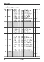
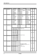
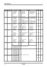
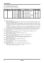
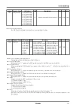
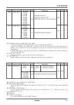
Address
Register Name
Bit Symbol
R/W
Description
H.Rst S.Rst B.Rst
0x70
IDE_CS00
7:
6:
Command Block Register
5:
4:
R/W
Data Register
0x00
0x00
–
3:
2:
1:
0:
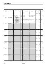
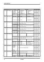
0x71
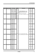
IDE_CS01
7:
6:
Command Block Register
5:
4:
R/W
Read : Error Register
0x00
0x00
–
3:
Write: Features Register
2:
1:
0:
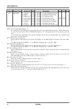
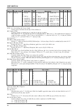
0x72
IDE_CS02
7:
6:
Command Block Register
5:
4:
R/W
Sector Count Register
0x00
0x00
–
3:
2:
1:
0:
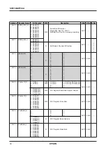
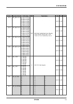
0x73
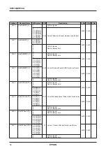
IDE_CS03
7:
6:
Command Block Register
5:
4:
R/W
Sector Number Register or
0x00
0x00
–
3:
Logical Block Address(LBA) bit 0 – 7
2:
1:
0:
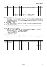
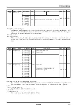
0x74
IDE_CS04
7:
6:
Command Block Register
5:
4:
R/W
Cylinder Low Register or
0x00
0x00
–
3:
Logical Block Address(LBA) bit 8 – 15
2:
1:
0:
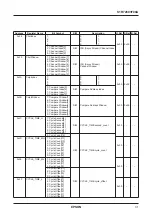
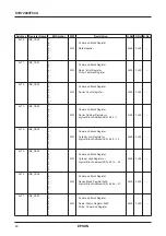
0x75
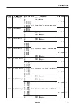
IDE_CS05
7:
6:
Command Block Register
5:
4:
R/W
Cylinder High Register or
0x00
0x00
–
3:
Logical Block Address(LBA) bit 16 – 23
2:
1:
0:
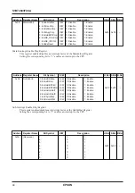
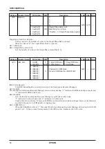
0x76
IDE_CS06
7:
6:
Command Block Register
5:
4:
R/W
Device/Head Register 0x00
0x00
0x00
–
3:
Logical Block Address(LBA) bit 24 – 27
2:
1:
0:
0x77
IDE_CS07
7:
6:
Command Block Register
5:
4:
R/W
Read : Status Register 0x00
0x00
0x00
–
3:
Write: Command Register
2:
1:
0:

