S1R72803F00A
50
EPSON
Address Register Name
Bit Symbol
R/W
Description
H.Rst S.Rst B.Rst
0x10
ChipCtl
7: Suspend
R/W
0: Resume
1: Suspend
6:
0:
1:
5:
0:
1:
4:
0:
1:
0x00
0x00
–
3:
0:
1:
2: IDE_MdlRst
W
0: None
1: IDE_Module Reset
1: SendTardy
R/W
0: None
1: Send Ack_tardy
0: SoftReset
W
0: None
1: Reset Start
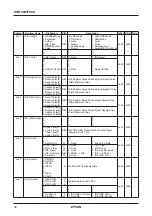
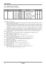
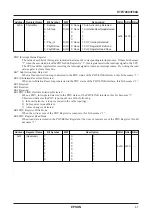
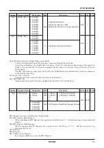
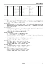
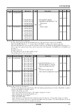
Chip Control Register
The Chip Ctl Register controls the internal circuit of a chip.
Bit7 Suspend
Setting this bit to “1” stops the Sclk supplied from the PHY to this IC. At that time, the LPS signal must be
negated as well.
When a LINKOn packet is received, the CPU asserts the xINT. After asserting it, the firmware asserts the LPS
signal to the PHY and resume it by the Sclk supplied from the PHY. At that time, this bit must be set to “0”.
Bit6 Reserved
Bit5 Reserved
Bit4 Reserved
Bit3 Reserved
Bit2 IDE_MdlRst
Setting this bit to “1” resets IDE-related registers (0x60 - 0x7F) to restore them to the initial state.
Bit1 Send Ack_tardy Enable
Makes setting to return an Ack_tardy as a Ack code when receiving an Async packet.
0: Usual Ack code
1: ack_tardy
Bit0 Soft Reset
Setting this bit to “1” initializes the interiors of the circuit. After initializing it, it is restored to “0”.
Address Register Name
Bit Symbol
R/W
Description
H.Rst S.Rst B.Rst
0x0E
PhyIntEnb
7: EnSubGap
R/W
0: Disable
1: Enable
6: EnArbGap
R/W
0: Disable
1: Enable
5:
0:
1:
4:
0:
1:
0x00
0x00
–
3:
0:
1:
2: EnPhy_int
R/W
0: Disable
1: Enable
1: EnPhyWrDone
R/W
0: Disable
1: Enable
0: EnPhyRdDone
R/W
0: Disable
1: Enable
Address Register Name
Bit Symbol
R/W
Description
H.Rst S.Rst B.Rst
0x0F
(Reserved)
7:
0:
1:
6:
0:
1:
5:
0:
1:
4:
0:
1:
0x00
0x00
–
3:
0:
1:
2:
0:
1:
1:
0:
1:
0:
0:
1:
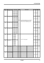
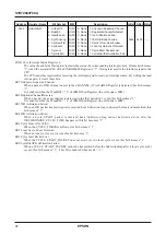
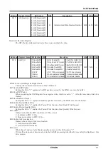
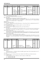
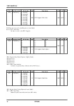
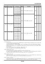
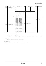
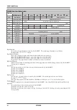
PHY Core Interrupt Enable Flag Register
This register enables/disables an interrupt factor of the PHYIntStat Register.
Setting the corresponding bit to “1” enables an interrupt to the CPU.


