S1R72803F00A
52
EPSON
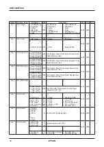
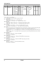
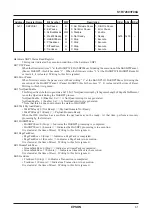
LINK Core Control Register Lower Rank
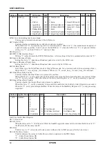
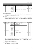
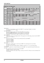
This register controls the functions of the LINK core.
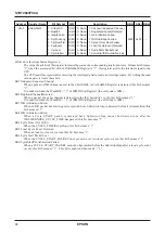
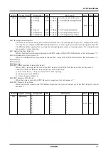
Bit7 Enable LINK
Controls whether communications with other nodes are enabled.
When this bit is “0”, no response is given to a received packet. When it is “1”, the transmission/reception of
a packet becomes possible. Even if you set the EnLINK to “1” when the LPS bit is “0”, it is ignored. Before
setting it to “1”, set the LPS bit to “1” and wait 10ms.
Bit6 Reserved
Bit5 PHY/LINK Interface Reset
Writing “1” to this bit resets the PHY/LINK interface. After resetting it, this bit is automatically restored to “0”.
Bit4 Ignore Broadcast Packet
Setting this bit to “1” abandons a Broadcast packet received by the LINK core.
Bit3 Ignore Broadcast Packet Data
Setting this bit to “1” abandons a Broadcast data received by he LINK core.
Bit2 Rx Busy Mode
Sets a Busy type, the Dual Phase mode or Single Phase mode, for a received packet when returning a Busy.
When this is “1”, an ack_busy_X is returned. When it is “0”, an ack_busy_A or ack_busy_B is returned.
Bit1 Dual Phase Retry Enable
Controls whether the Dual Phase retry protocol is enabled.
When this bit is “1”, a retry processing is done until a time set on the Retry Limit Register is exceeded. When
it is “0”, no retry is done. When the value of the Retry Limit Register is “0”, a retry processing is ignored.
Bit0 Single Phase Retry Enable
Controls whether the Single Phase retry protocol is enabled.
When this bit is “1”, a retry processing is done until the number set on the Retry Limit Register is exceeded.
When it is “0”, a retry processing is disabled. When the value of the MaxRetry Register is “0”, a retry processing
is ignored.
Address Register Name
Bit Symbol
R/W
Description
H.Rst S.Rst B.Rst
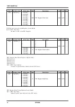
0x19
LinkCtl_L
7: EnLink
R/W
0: Disable Link
1: Enable Link
–
–
6:
0:
1:
–
–
5: PLIFrst
W
0: None
1: Reset PHY/Link I/F
0
–
4: IgnrBChdr
R/W
0: BC Pkt to DMA FIFO 1: Ignore BC Packet
0x00
0
–
3: IgnrBCdata
R/W
0: BC Data to DMA FIFO 1: Ignore BC – Data
0
–
2: RxBusyMode
R/W
0: Dual
1: Single
0
–
1: DualRtyEnb
R/W
0: Dual Retry Disable 1: Dual Retry Enable
0
–
0: SinglRtyEnb
R/W
0: Single Retry Disable 1: Single Retry Enable
0
–
Address Register Name
Bit Symbol
R/W
Description
H.Rst S.Rst B.Rst
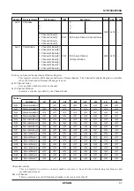
0x1A
LinkStart
7:
0:
1:
6:
0:
1:
5:
0:
1:
4:
0:
1:
0x00
–
–
3:
0:
1:
2: ID_Valid
R
0: PhyID Invalid
1: PhyID Valid
1: Root
R
0: Self Node =Not Root
1: Self Node =Root
0: CablPwSts
R
0: Cable Power Status NG
1: Cable Power Status OK
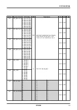
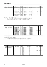
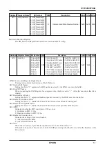
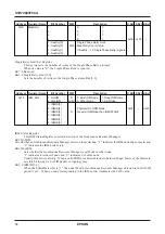
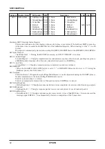
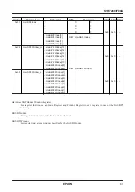
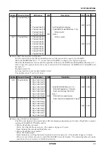
Link Core Status Read Register
Bit 7..3 Reserved
Bit2 ID_Valid
When this bit is set to “1,” the Physical_ID of the NodeID register becomes valid, and when this bit is set to “0,”
the Physical_ID becomes invalid.
Bit1 Root
This bit is set to “1” when the self node comes to Root in the Self-ID process after the bus is reset.
Bit 0 Cable Power Status
This bit indicates the status of Cable Power, which is updated in the PHY Status.
“1” : Cable Power Status OK
“0” : Cable Power Status NG

