S1R72803F00A
70
EPSON
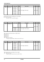
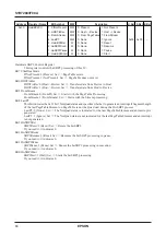
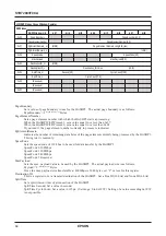
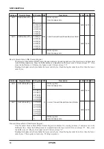
Address
Register Name
Bit Symbol R/W
Description
H.Rst S.Rst B.Rst
0x4E
IDE_TxStreamPtr_H 7:
Write is ignore
6:
Read is always zero
5:
4: ITSP[12]
0x00
0x00
–
3: ITSP[11]
2: ITSP[10]
1: ITSP[9]
0: ITSP[8]
0x4F
IDE_TxStreamPtr_L 7: ITSP[7]
R/W Transmit Packet Stream Data Area IDE Pointer
6: ITSP[6]
5: ITSP[5]
4: ITSP[4]
0x00
0x00
–
3: ITSP[3]
2: ITSP[2]
1:
Write is ignore
0:
Read is always zero
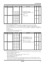
Address
Register Name
Bit Symbol R/W
Description
H.Rst S.Rst B.Rst
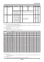
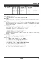
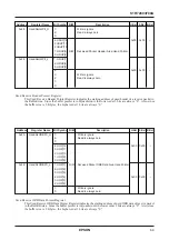
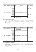
0x4C
IDE_RxStreamPtr_H 7:
Write is ignore
6:
Read is always zero
5:
4: IRSP[12]
0x00
0x00
–
3: IRSP[11]
2: IRSP[10]
1: IRSP[9]
0: IRSP[8]
0x4D
IDE_RxStreamPtr_L 7: IRSP[7]
R/W
Received Packet Stream Data Area IDE Pointer
6: IRSP[6]
5: IRSP[5]
4: IRSP[4]
0x00
0x00
–
3: IRSP[3]
2: IRSP[2]
1:
Write is ignore
0:
Read is always zero
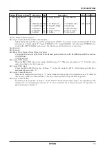
Receive Stream Data IDE Pointer Register
This Receive Stream Data IDE Pointer Register indicates the starting address of received stream data in the
RxSTreamArea that is to be transmitted to the IDE side but not yet transmitted. Since the buffer pointer is in
Quadlet unit, the lower order 2 bits are always “0”. Also, since the buffer size is 2 Kbytes, the higher order 3
bits are always “0”.
Reading the higher order bytes holds the lower order bytes. Read the higher order bytes first, then the lower
order bytes.
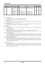
Transmit Stream Data IDE Pointer Register
This Transmit Stream Data IDE Pointer Register indicates the starting address of stream data in the
RxStreamArea to be stored following the data that was transmitted from the IDE to the SRAM. Since the buffer
pointer is in Quadlet unit, the lower order 2 bits are always “0”. Also, since the buffer size is 2 Kbytes, the higher
order 3 bits are always “0”.
Reading the higher order bytes holds the lower order bytes. Read the higher order bytes first, then the lower
order bytes.

