S1R72803F00A
80
EPSON
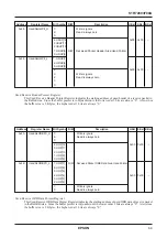
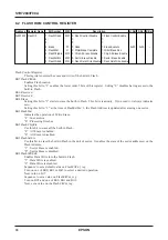
IDE Configuration Register
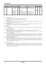
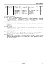
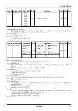
This register sets the mode of operation of the IDE interface of this IC.
Bit7 IDE_Reset
Writing “1” to this bit asserts the RESET signal to the IDE interface for 50
µ
s. During asserting the XHRESET,
this bit reads “1”. If you reset it during the assertion, the XHRESET is output for 50
µ
s from that time.
Bit6::3 Reserved
Bit2 XDIOW_DLYen
XDIOW is delayed by one clock (20 ns) as compared with XDMACK on Multiword DMA.
Bit1::0 Reserved
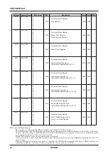
Address
Register Name
Bit Symbol
R/W
Description
H.Rst S.Rst B.Rst
0x62
IDE_RegAccCyc 7: Assert Pulse[3]
6: Assert Pulse[2]
R/W IDE Register Access Strobe Signal Assert Pulse
5: Assert Pulse[1]
Width Minimum Value
4: Assert Pulse[0]
0x00
0x00
–
3: Negate Pulse[3]
2: Negate Pulse[2] R/W IDE Register Access Strobe Signal Negate Pulse
1: Negate Pulse[1]
Width Minimum Value
0: Negate Pulse[0]
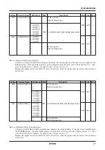
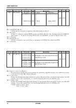
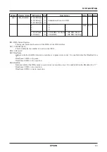
IDE Register Access Cycle Register
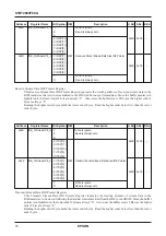
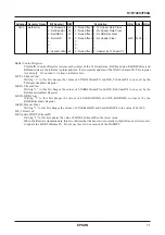
This register sets a transfer mode when accessing the register area of the IDE interface. It is enabled for an access
to 0x70 to 0x7F of the IDE-CS0/CS1 Register.
Bit7::4 Assert Pulse
Decides the minimum value of the assert period of the strobe signal when accessing the register area of the IDE
interface. It is a value [Assert Pulse + 2] times the internal operation clock (50MHz) cycle.
Bit3::0 Negate Pulse
Decides the minimum value of the negate period of the strobe signal when accessing the register area of the IDE
interface. It is a value [Assert Pulse + 2] times the internal operation clock (50MHz) cycle.
Example: 0000: 2 x 20ns = 40ns
0001: 3 x 20s = 60ns
Address Register Name
Bit Symbol
R/W
Description
H.Rst S.Rst B.Rst
0x61
IDE_Config1
7: IDE_Reset
R/W
0: None
1: IDE Reset
6:
0:
1:
5:
0:
1:
4:
0:
1:
0x00
0x00
–
3:
0:
1:
2: XDIOW_DLYen R/W
0: None
1: Delay XDIOW
1:
0:
1:
0:
0:
1:

