S1R72803F00A
86
EPSON
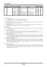
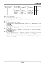
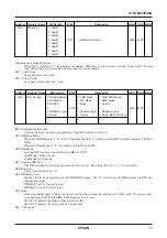
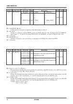
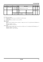
IDE Command Block Register
This register is a Command Block Register that is the I/O port of the IDE interface.
The transfer mode of the Data Register is PIO mode-fixed, having access based on conditions set on the IDE_PioDmaCyc
Register. Since the setting at the BUS8/SWAP bit of the CONFIG Register is reflected, 16-bit access is possible by always
accessing the Data Register twice if it is 16 bits wide.
During DMA transfer, access to the Data Register is disabled.
If you access the 0x71-0x77 in the DMA mode or when the InterLock bit is not on, the HDMARQ is negated once and CPU
access is done.
When the Interlock bit is on or at the time of UltraDMA, the XHDMACK is negated at the time of HDMAQR off or on
completion of transfer. Note that, for this reason, the CPU access is put in wait state.
Address
Register Name
Bit Symbol
R/W
Description
H.Rst S.Rst B.Rst
0x70
IDE_CS00
7:
6:
Command Block Register
5:
4:
R/W
Data Register
0x00
0x00
–
3:
2:
1:
0:
0x71
IDE_CS01
7:
6:
Command Block Register
5:
4:
R/W
Read : Error Register
0x00
0x00
–
3:
Write: Features Register
2:
1:
0:
0x72
IDE_CS02
7:
6:
Command Block Register
5:
4:
R/W
Sector Count Register
0x00
0x00
–
3:
2:
1:
0:
0x73
IDE_CS03
7:
6:
Command Block Register
5:
4:
R/W
Sector Number Register or
0x00
0x00
–
3:
Logical Block Address(LBA) bit 0 – 7
2:
1:
0:
0x74
IDE_CS04
7:
6:
Command Block Register
5:
4:
R/W
Cylinder Low Register or
0x00
0x00
–
3:
Logical Block Address(LBA) bit 8 – 15
2:
1:
0:
0x75
IDE_CS05
7:
6:
Command Block Register
5:
4:
R/W
Cylinder High Register or
0x00
0x00
–
3:
Logical Block Address(LBA) bit 16 – 23
2:
1:
0:
0x76
IDE_CS06
7:
6:
Command Block Register
5:
4:
R/W
Device/Head Register 0x00
0x00
0x00
–
3:
Logical Block Address(LBA) bit 24 – 27
2:
1:
0:
0x77
IDE_CS07
7:
6:
Command Block Register
5:
4:
R/W
Read : Status Register 0x00
0x00
0x00
–
3:
Write: Command Register
2:
1:
0:

