Chapter 4 Technical Description
18
EPSON
S5U13719P00C100 Evaluation Board User Manual (Rev. 1.1)
4.6 Camera Interface
All the signals for the Camera1 interface are available on connector H3. All the signals for the Camera2 interface
are available on connector H7.
Camera modules are programmed using an I2C type bus. The S1D13719 does not have an I2C interface, but it has
GPIOs that can be used to emulate the I2C bus. By default, the board uses GPIO17 as SCL signal of I2C bus and
GPIO18 as SDA signal of I2C bus. If GPIO17 and GPIO18 must be used for some other function, for example SD
Card interface, than GPIO1 can be selected for SCL by removing R38 and populating R37 with a 0
Ω
resistor, size
0402. GPIO2 can be selected for SDA by removing R44 and populating R43 with a 0
Ω
resistor, size 0402.
The I2C bus lines must be pulled high. The default configuration of the evaluation board has the I2C lines, SCL and
SDA, pulled high to CIO1VDD. If the I2C lines must be pulled high to CIO2VDD, R34 and R41 must be removed
and 2.2k
Ω
resistors, size 0402, must be mounted for R35 and R42.
The reset signal provided on H3 and H7 is active low and is pulled to HIOVDD when inactive.
The S1D13719 camera interface has a strobe output, CMSTROUT, that is available on H6 connector. Note that
connector H6 is not populated on the S5U13719P00C100 evaluation board.
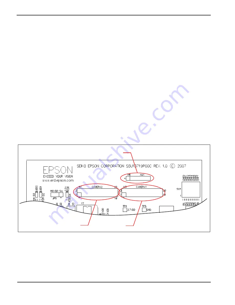
The following diagram shows the location of the camera connectors H3, H6 and H7. H3 and H7 are 0.1x0.1”, 20-
pin headers (10x2). H6 is 0.1”, 6-pin header (6x1).
Figure 4-4: Camera Expansion Connector Locations (H3, H6 and H7)
For the pinout of connectors H3, H6 and H7, see Section Chapter 6, “Schematic Diagrams” on page 23.
H7
H3
H6


