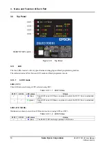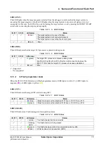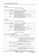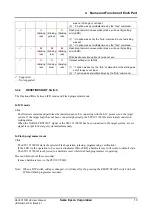
3. Name and Function of Each Part
S5U1C17001H2 User Manual
Seiko Epson Corporation
5
(ICDmini Ver2.0) (Rev2.0)
3. Name and Function of Each Part
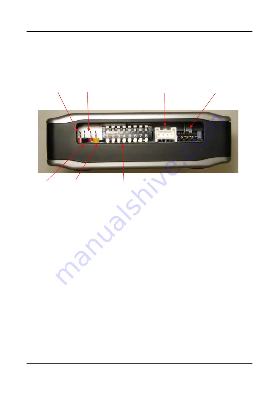
The following shows the name of each part of the S5U1C17001H.
3.1 Left
Side
Panel
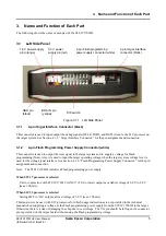
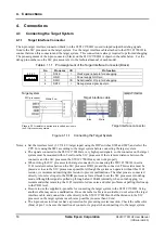
Figure 3.1.1 Left Side Panel
3.1.1
4-pin Target Interface Connector (black)
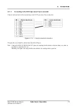
This connector is used to input/output the debug signals (DCLK, DSIO, and DST2) from/to the S1C processor on
the target system. See Section 4.1.1, “Target Interface Connector,” for the pin assignment and connection.
3.1.2
4-pin Flash Programming Power Supply Connector (white)
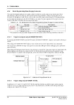
This connector is used to output the reset signal to the target system and to supply a voltage for Flash
programming (Note). Also it is used to input the target operating voltage when the target system voltage level is
used for the debug signal interface. See Section 4.1.2, “Flash Programming Power Supply Connector,” for the pin
assignment and connection.
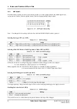
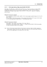
Note: The S5U1C17001H includes a Flash programming power supply
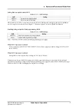
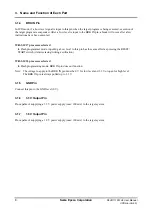
When S1C17 processor is selected
Use in conjunction with S5U1C17001C (GNU17 v2.0.0 or later) outputs a variable voltage of 6.0 V to 8.0 V
(max. 100 mA).
When S1C33 processor is selected
Setting SW8 to “On” outputs a fixed voltage of 7.0 V (max. 100 mA).
This must never be used with S1C processors for which usage instructions are not provided in the technical
manual when supplying a voltage as the Flash programming power supply from the S5U1C17001H to the target.
Otherwise, there is a risk of damaging the chip due to overvoltage. The V
PP
pin should be left open if a connector
pin is provided on the target board without using the Flash programming voltage.
BRK IN pin
(yellow)
DIP switch
4-pin Flash programming
power supply connector (white)
4-pin target interface
connector (black)
1.8 V power supply
pin (orange)
3.3 V power
supply pin (red)
GND pin
(black)


