background image

6. Flash 

Programmer 

Mode 


26  

Seiko Epson Corporation


S5U1C17001H2 User Manual 

(ICDmini Ver2.0)   


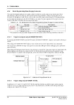
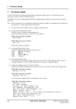
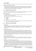
Example:  With S1C processor that supports sector erasing 

To erase sectors 0 to 31 and load user_program.saf from Flash 0x8000 address 
Specify sector  1 when specifying erase start/end blocks. 
(gdb) c17  fwld  user_program.saf  1  32  0x8000 


The procedure for specifying the sectors for erasing will differ depending on the S1C17 model. For details of 
the particular method, refer to the “ReadMe” shown below created when the GNU17 was installed. 

User folder

\EPSON\GNU17\mcu_model\model\fls\ 


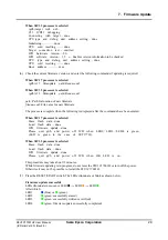
When S1C33 is selected 

Example:  To erase all sectors and load user_program.saf from Flash 0xc00000 address 

(gdb) c33  fwld user_program.saf  0  0  0xc00000 


Example:  To erase sectors 0 to 141 and load user_program.saf from Flash 0xc00000 address 

Specify the corresponding sector number when specifying erase start/end blocks. 
(gdb) c33  fwld  user_program.saf  0  141  0xc00000 


For more details of fwld commands, refer to the documentation included with the FLS program. 
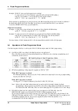
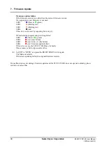
 

6.2 

Operations in Flash Programmer Mode 

The following describes how to start up the S5U1C17001H and procedure for Flash programming. 


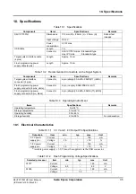
(1)  Set SW2 and SW3 according to the Flash operation to be performed. 

One of the three sequences, erasing and programming, verification only, or erasing, programming, and 
verification, can be selected. 

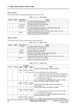
Table 6.2.1  DIP Switch Settings in Flash Programmer Mode   

SW2 SW3 

Setting 

OPEN (

) OPEN 

(

ICD mode (default) 

ON (

) OPEN 

(

Flash programmer mode     Erase 

 program 

OPEN (

) ON 

(

Flash programmer mode     Verify 

ON (

) ON 

(

Flash programmer mode     Erase 

 program 

 verify 


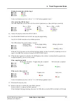
(2)  If Flash programming voltage output is required, set SW8 to “ON.”


When S1C17 processor is selected 

The Flash programming voltage set by the “fwlp” command is output only for erasing or programming 
from the FLASH VCC OUT pin. 


When S1C33 processor is selected 

A voltage of 7 V is output continuously from the FLASH VCC OUT pin. 

 
Note:  Refer to the individual technical manual for each model to determine whether the Flash 

programming voltage supply is required. Do not use this voltage unless specifically mentioned in 
the technical manual. Otherwise, there is a risk of damaging the S1C processor due to overvoltage. 


(3)  If the DIP switches have been altered while power is supplied via the USB cable, press the 

RESET/START switch to switch the S5U1C17001H to Flash programmer mode. 
If you change the DIP switch settings with the power off, connect the USB cable of the ICDmini to the 
USB port of the host computer or to a 5 V AC USB adapter (see “3.2 Right Side Panel”) to supply power. 
In the Flash programmer mode, only power is required from the USB cable and there is no 
communication with the host computer. 
 

Summary of Contents for S5U1C17001H2

Page 1: ...Rev 1 1 CMOS 16 BIT SINGLE CHIP MICROCONTROLLER S5U1C17001H2 User Manual ICDmini Ver2 0 ...

Page 2: ...n Seiko Epson reserves the right to make changes to this material without notice Seiko Epson does not assume any liability of any kind arising out of any inaccuracies contained in this material or due to its application or use in any product or circuit and further there is no representation that this material is applicable to products requiring high level reliability such as medical products Moreo...

Page 3: ... 0P TCP ST 4 directions 0Q TCP SD 4 directions 0R Tape reel RIGHT 99 Specs not fixed Specification Package D die form F QFP B BGA Model number Model name C microcomputer digital products Product classification S1 semiconductor Packing specifications 00 standard packing Version 1 Version 1 Tool type Hx ICE Dx Evaluation board Ex ROM emulation board Mx Emulation memory for external ROM Tx A socket f...

Page 4: ...1 Target Interface Connector 14 4 1 1 1 Connecting to the S1C33 processor 10 pin connector 15 4 1 2 Flash Programming Power Supply Connector 16 4 1 2 1 Target reset signal output TARGET RST OUT 16 4 1 2 2 Target voltage input TARGET VCC IN 16 4 1 2 3 Flash programming voltage output FLASH VCC OUT 17 4 2 Connecting to the Host Computer 18 4 2 1 USB Driver Locations 18 4 2 2 USB Driver Installation ...

Page 5: ...e Update 28 8 Precautions 31 8 1 Restrictions on Debugging 31 8 2 Differences from the Actual IC 32 8 3 Notes on Use of S5U1C17001H 32 8 4 Differences between the S5U1C17001H and S5U1C33001H 33 9 Troubleshooting 34 10 Specifications 35 10 1 Electrical Characteristics 35 Appendix 36 Initial Validation when Designing a Target System 36 Revision History 38 ...

Page 6: ...ons depending on the ICD cannot be used This is the mode to debug the target program using the S5U1C17001H ICDmini or S5U1C17002H ICD board The program will be executed on the target system The S5U1C17001H ICDmini must be used in this mode Target S1C17xxx Normal mode Debug mode The normal mode is the normal state while the target system is executing the user program The target enters debug mode by...

Page 7: ...l C Compiler Package for S1C17 Family or S5U1C33001C Manual C Compiler Package for S1C33 Family Figure 1 1 S5U1C17001H External View Note Do not open the case as it may cause a malfunction This manual applies to the following S5U1C17001H2100 ICDmini ver2 0 S5U1C17001H S1C17 firmware ver3 2 S1C33 firmware ver1 5 1 1 Products may be shipped installed with later versions than those indicated above du...

Page 8: ...s and 6515 hours In second units 3 µs to 36 minutes In s units 3 s to 1 8 minutes Cycle counting function Not available Available Standalone Flash programmer function Available Firmware update function Available DCLK frequency to communicate with the target 1 4 kHz to 40 MHz 2 4 kHz to 40 MHz Flash programming power voltage supply Available Variable voltage output 6 0 V to 8 0 V max 100 mA Availab...

Page 9: ... Fixed 7 0 V voltage max 30 mA output with S1C33 processor selected Fixed 7 0 V voltage max 30 mA output with S1C33 processor selected 1 Flash programming voltage supply to Vpp pin Not supported Not supported Supported Supported target system I O voltage 3 3 V 1 8 V or voltage input from target 1 0 V to 5 0 V 3 3 V 1 8 V or voltage input from target 1 0 V to 5 5 V 3 3 V 1 8 V or voltage input from...

Page 10: ...oad guide English Japanese 1 each The items specified below are not included with the package These items must be prepared separately When developing an S1C17 application S5U1C17001C S1C17 Family C Compiler Package S1C17 Family debugger gdb included with package S5U1C17001C Manual Included with S1C17 Family C Compiler Package When developing an S1C33 application S5U1C33001C S1C33 Family C Compiler...

Page 11: ...erface See Section 4 1 2 Flash Programming Power Supply Connector for the pin assignment and connection Note The S5U1C17001H includes a Flash programming power supply When S1C17 processor is selected Use in conjunction with S5U1C17001C GNU17 v2 0 0 or later outputs a variable voltage of 6 0 V to 8 0 V max 100 mA When S1C33 processor is selected Setting SW8 to On outputs a fixed voltage of 7 0 V ma...

Page 12: ...ngs SW2 SW3 Setting OPEN OPEN ICD mode default ON OPEN Flash programmer mode Erase program OPEN ON Flash programmer mode Verify ON ON Flash programmer mode Erase program verify ICD mode Mode for executing debugging commands from the debugger on the host computer For more information on this mode refer to 5 ICD Mode Flash programmer mode The S5U1C17001H operates as a standalone Flash programmer For...

Page 13: ... 3 1 3 6 SW8 Settings SW8 Setting OPEN Stop Flash programming voltage default ON Output Flash programming voltage Note The S5U1C17001H includes a Flash programming power supply When S1C17 processor is selected Use in conjunction with S5U1C17001C GNU17 v2 0 0 or later outputs a variable voltage of 6 0 V to 8 0 V max 100 mA When S1C33 processor is selected Setting SW8 to On outputs a fixed voltage o...

Page 14: ...mode inputting a Low level to this pin has the same effect as pressing the RESET START switch it starts erasing writing verification With S1C33 processor selected In Flash programming mode BRK IN pin does not function Note The voltage to apply to the BRK IN pin must be 0 V for low level and 3 3 V or open for high level The BRK IN pin is always pulled up to 3 3 V 3 1 5 GND Pin Connect this pin to t...

Page 15: ...te When a bus powered USB hub is used to connect the S5U1C17001H to the host computer there may be a shortage of drive power Especially if supplying the flash programming voltage either connect directly to the host computer s USB port or use an AC adapter with USB 5 V output capable of supplying power to the USB cable If using an AC adapter set the S5U1C17001H mode to be used and confirm beforehan...

Page 16: ...1 In ICD mode LED1 CPU This LED indicates the target CPU selected using SW1 Table 3 3 1 1 1 LED1 Status S1C17 S1C33 LED status Status blue Target CPU is an S1C17xxx or a product in which the S1C17 Core is embedded C17 green Target CPU is an S1C33xxx or a product in which the S1C33 Core is embedded C33 LED2 ICD MODE Illuminates as shown below when ICD mode is selected using SW2 and SW3 Table 3 3 1 ...

Page 17: ...D4 Status S1C17 S1C33 LED status Status green The target S1C processor is placed in debug mode Also this LED rights with LED3 before the initial connection between the S5U1C17001H and the target S1C processor has been established out Other Supported Not supported 3 3 1 2 In Flash programmer mode When the S5U1C17001H starts up in Flash programmer mode LED2 lights in white LED3 lights in magenta or ...

Page 18: ...operation has completed normally OK green Write back completed successfully OK Blinks when flash programmer mode non execution option n is set A Flash verify error has occurred ERR red Write back completed successfully OK Table 3 3 1 2 5 Other Errors LED status S1C17 S1C33 LED1 LED2 LED3 Status blinking red blinking red blinking magenta Flash programming voltage setting error ERR The error conditi...

Page 19: ...ESET RESTART Switch The function differs between ICD mode and Flash programmer mode In ICD mode Click The firmware restarts and performs the initial sequence for connecting with the S1C processor on the target system If the target board has not been connected physically the S5U1C17001H enters initial connection waiting status When the TARGET RST OUT signal of the S5U1C17001H has been connected to ...

Page 20: ...distance between the connector and the S1C processor the S5U1C17001H may not work properly When wiring the S1C processor to the target connector for connecting the S5U1C17001H insert a 33 resistor in series between the S1C processor DSIO pin and the connector This resistor must be placed as close to the S1C processor as possible Although the system can operate without this 33 resistor we recommend...

Page 21: ...or pin NO 4 pin connector pin 1 DCLK 1 DCLK 2 GND 2 GND 3 DSIO 3 DSIO 4 GND 4 DST2 5 DST2 6 GND 7 DST1 8 GND 9 DST0 10 DPCO Figure 4 1 1 2 10 pin Connector Connection The pins above not linked by dotted lines should be left open Note Connect the S5U1C17001H to the S1C processor ensuring that the distance between them is as short as possible no more than 20 cm Shielding the signal wire using GND is...

Page 22: ...r of the target interface connector 4 1 2 1 Target reset signal output TARGET RST OUT By pressing the RESET START switch in ICD mode the TARGET RST OUT outputs a reset signal to the target system When using the TARGET RST OUT output a reset circuit as shown in the figure below is recommended The connection to RESET of target reset signal is not essential although it allows debugging to be performe...

Page 23: ... or later outputs a variable voltage of 6 0 V to 8 0 V max 100 mA For more details of the Flash programming voltage output method with the S1C17 processor selected refer to 5 4 Flash Programming Voltage Setting or 6 Flash Programmer Mode When S1C33 processor is selected Setting SW8 to ON outputs a fixed voltage of 7 0 V max 100 mA Setting SW8 to ON always outputs a voltage of 7 V voltage from the ...

Page 24: ...17 processor is selected The USB driver is located in the following directory created when the S5U1C17001C GNU17 was installed User Folder EPSON GNU17 utility drv_usb When S1C33 processor is selected The USB driver is located in the following directory created when the S5U1C33001C GNU33 was installed User Folder EPSON GNU33 utility drv_usb Icd33v60 4 2 2 USB Driver Installation Procedure Install t...

Page 25: ...2 1 USB Driver Locations When S1C17 processor is selected When S1C33 processor is selected Figure 4 2 2 2 Driver Installation Screen The device manager will be displayed as shown below when the USB driver has been installed correctly When S1C17 processor is selected When S1C33 processor is selected Figure 4 2 2 3 Driver Installation Complete Screen Note If the window above is not displayed correct...

Page 26: ...nabled by pressing the RESET START switch 5 2 Activation in ICD Mode After connecting the S5U1C17001H to the target system and the host computer start up the S5U1C17001H by following the procedure described below If the S5U1C17001H is started up in another procedure it may not be connected to the target system normally 5 2 1 When the TARGET RST OUT Signal is Not Connected When the TARGET RST OUT s...

Page 27: ...lue or green LED2 blue LED3 red LED4 green or out 5 3 Starting Up the Debugger Start up the debugger gdb on the host computer after the connection between the S5U1C17001H and the target S1C processor has been established by the operations described above When debugging using the debugger with the S5U1C17001H connected the debugger must be set to each mode by executing the target command When the S...

Page 28: ...oltage settings The Flash programming voltage settings can be set using the following commands after the S5U1C17001H and debugger gdb have been started up The Flash programming voltage will differ depending on the model For more details on the Flash programming voltage refer to the corresponding technical manual Flash erasing programming voltage setting and output start gdb c17 flv Voltage Voltage...

Page 29: ...ernal Flash memory to the S5U1C17001H internal memory using the debugger gdb fwlp command 4 Load the data to be written to the target Flash memory to the S5U1C17001H using the fwld command 5 Quit the debugger For details of debugger gdb start end procedures and how to create saf format files refer to the S5U1C17001C Manual S1C17 Family C Compiler Package or the S5U1C33001C Manual S1C33 Family C Co...

Page 30: ...ine address ProgramSize Write back FLS program size Parameters WriteBackEntryAddr 0x000000 WriteBackEntryAddr 0xfffffe hexadecimal ProgramSize 0000 ProgramSize 8192 base 10 n Function Flash programmer mode non execution option Specifying the n option within the comment section allows the flash programmer functions erase write and verify not to be executed This option is used in conjunction with th...

Page 31: ...8 b0x10 1312 For more details of FLS programs such as erasing and writing routine addresses refer to the ReadMe shown below created when the GNU17 was installed User folder EPSON GNU17 mcu_model model fls When S1C33 processor is selected Example Save FLS program fls_program saf to S5U1C17001H internal memory With erasing routine address 0x14c and writing routine address 0x180 gdb c33 fwlp fls_prog...

Page 32: ...e three sequences erasing and programming verification only or erasing programming and verification can be selected Table 6 2 1 DIP Switch Settings in Flash Programmer Mode SW2 SW3 Setting OPEN OPEN ICD mode default ON OPEN Flash programmer mode Erase program OPEN ON Flash programmer mode Verify ON ON Flash programmer mode Erase program verify 2 If Flash programming voltage output is required set ...

Page 33: ...ng verification ERASE blinking white WRITE blinking magenta VERIFY blinking yellow When the S1C17 processor is selected the Flash programmer can also be started by inputting a low level signal to the BRK IN pin instead of using the RESET START switch 6 When the Flash operation has finished the LED lights as shown below to indicate that the operation has completed normally or an error has occurred ...

Page 34: ...witches to OPEN 3 Press the RESET START switch The S5U1C17001H LEDs illuminate as shown below LED1 blue or green LED2 blue LED3 red or out LED4 green 4 Start up the debugger gdb For details of how to start the debugger gdb refer to the S5U1C17001C Manual S1C17 Family C Compiler Package or S5U1C33001C Manual S1C33 Family C Compiler Package 5 Connect the debugger gdb to the S5U1C17001H Execute the f...

Page 35: ...e saf File name for new firmware The process is complete when the following is displayed after the commands have been entered When S1C17 processor is selected Erase flash data done Load flash data done ICD firmware update done Please quit gdb and power off ICD when LED2 LED3 LED4 is green LED is green in the case of SVT17701 When S1C33 processor is selected Erase flash data done Load flash data do...

Page 36: ... from step 1 If Flash erasing programming verifying failed LED1 blue or green LED2 red erase failed LED3 red write or verify failed LED4 red firmware update failed If this error occurs the S5U1C17001H may be faulty Please contact a Seiko Epson sales office 8 Set SW7 to OPEN and press the RESET START switch again The firmware restarts If firmware updating failed the original firmware restarts If a ...

Page 37: ... received in other parts of the program is paused as with the STEP command The interrupt that has been paused is serviced immediately before the target program is executed or immediately after one instruction is executed after the debugger gdb on the host computer has directed that the target program be executed For details on single step execution STEP and NEXT refer to the Debugger section in th...

Page 38: ...cting the target system The signals connected to the S5U1C17001H are very high speed signals so the connector on the target system must be mounted within 5 cm from the target S1C processor If there is more distance between the connector and the S1C processor the S5U1C17001H may not work properly Furthermore be sure to use the supplied 4 pin cable for connecting the target system to the S5U1C17001H...

Page 39: ...fail if voltages that exceed this range are input Therefore target systems to be connected to the S5U1C17001H must be designed so that voltages outside this range are not applied Take special care in designing the target system power supply and design the target system so that over voltages are not applied to the S5U1C17001H when the target system power supply is turned on or off 8 4 Differences b...

Page 40: ...running See Section 5 2 Activation in ICD Mode and start up in the correct order The following message suddenly appears while the target program is being executed by the debugger gdb in the host computer Break by external break Program received signal SIGINT Interrupt This problem is caused by low level noise on the DSIO signal of the target system or when the BRK IN pin goes GND level 1 Is the ta...

Page 41: ...2 4PA 2 54DS 71 HRS Flash programming power supply connector 4 pins white Connector 4 pin L angle S04B PASK 2 JST Flash programming power supply connector 4 pin black Connector 4 pin straight A2 4PA 2 54DS 71 HRS Table 10 3 Operating Environment Items Specifications Remarks Operating temperature 5 to 35 C Storage temperature 10 to 60 C Operating humidity 35 to 80 Storage humidity 20 to 90 No conde...

Page 42: ...signal is input continuously the output from DST2 is as follows DST2 If DST2 pin output pin does not change from Low to High check the hardware of the target system Step 2 Try to establish a connection with the S5U1C17001H 1 Set the DIP switches of the S5U1C17001H The default is all open Set the switches appropriately for the target system In this test make the following settings at the minimum SW...

Page 43: ...7001H2 User Manual Seiko Epson Corporation 37 ICDmini Ver2 0 Rev2 0 LED1 blue or green LED2 blue LED3 red LED4 out Press the RESET START switch on the S5U1C17001H once and input High Low High signals to the RESET pin ...

Page 44: ...ew 411153403 Page 3 Error corrected S5U1C17001T S5U1C17001H Pages 1 3 Page 3 Page 9 Pages 12 13 Pages 23 27 Pages 28 30 Firmware version changed Operating system description changed AC adapter usage description changed fwlp command option s b n and t descriptions added fwlp command option s b n and t descriptions added Firmware update function changed ...

Page 45: ...8057 CHINA Phone 86 755 2699 3828 FAX 86 755 2699 3838 EPSON HONG KONG LTD Unit 715 723 7 F Trade Square 681 Cheung Sha Wan Road Kowloon Hong Kong Phone 852 2585 4600 FAX 852 2827 4346 EPSON TAIWAN TECHNOLOGY TRADING LTD 14F No 7 Song Ren Road Taipei 110 TAIWAN Phone 886 2 8786 6688 FAX 886 2 8786 6660 EPSON SINGAPORE PTE LTD 1 HarbourFront Place 03 02 HarbourFront Tower One Singapore 098633 Phone...

Page 46: ...Mouser Electronics Authorized Distributor Click to View Pricing Inventory Delivery Lifecycle Information Epson S5U1C33001H1400 ...

Reviews: