4. Connector
S5U1C17564T Manual
Seiko Epson Corporation
13
(Rev.1.0)
4.1.2
Debug interface connector (J5 - J6)
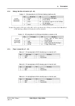
Table 4.5 Pin assignment of CPU board debug interface (J5)
No.
Pin name
I/O
Function
1
DCLK
O
Clock signal for debugging
2 GND
- Power (GND)
3 DSIO
I/O Input/Output
signal for serial interface
for debugging
4
DST2
O
Debug status signal
Caution! The position of the pin 1 of the CN2-1 (J5) is as shown above. When you connect the ICDminiVer.2
to this board, pay attention to the direction of the connector.
Table 4.6 Pin assignment of CPU board interface connector (J6)
No.
Pin name
I/O
Function
1 VPP
I
Power input for flash memory
programming
2 GND
- Power
(GND)
3
RESET
I
Reset signal input for the target
4 VCCIN
O Target
voltage
output
4.1.3
Power connector (J7 - J9)
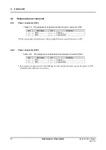
Table 4.7 Pin assignment of CPU board power connector (J7)
No.
Pin name
I/O
Function
1 HVDD
-
Power(+)
2 GND
-
Power(GND)
Table 4.8 Pin assignment of CPU board power connector (J8)
No.
Pin name
I/O
Function
1 LVDD
- Power(+)
2 GND
- Power(GND)
Table 4.9 Pin assignment of CPU board power connector (J9)
No.
Pin name
I/O
Function
1 AVDD
- Power(+)
2 GND
- Power(GND)
4 3 2 1
1 2 3 4

