background image

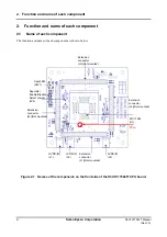
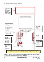
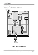
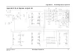
2.  Function and name of each component 


S5U1C17564T Manual


Seiko Epson Corporation

 5 

(Rev.1.0)


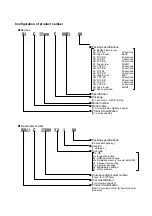
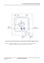
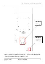
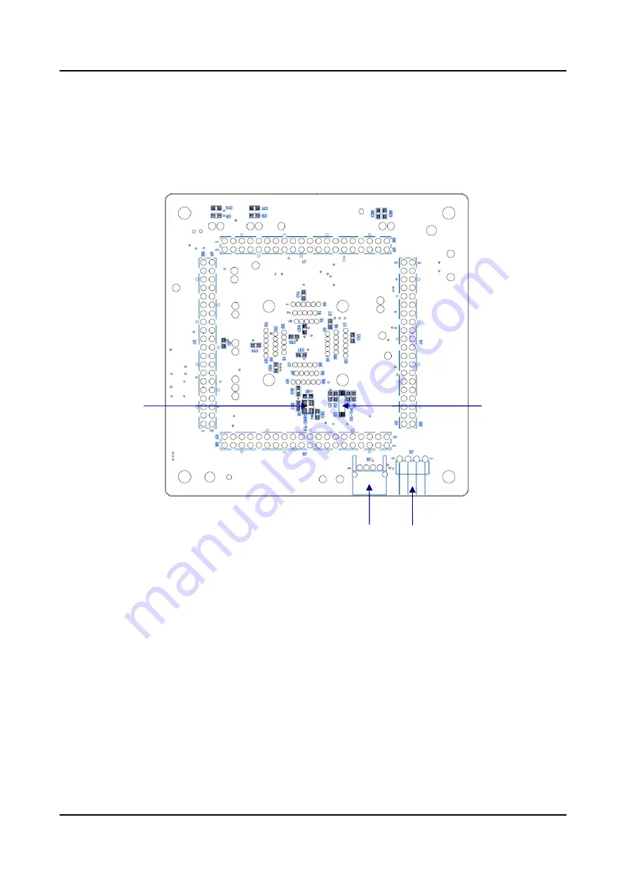
Figure 2.2    Names of the components on the back side of the S5U1C17564T1 CPU board. 


Caution!      The position of the pin 1 of the CN2-1 (J5) is as shown above. When you connect the 

ICDminiVer.2 to this board, pay attention to the direction of the connector. 


32.768kHz  
Crystal Unit (X2)

12MHz  
Crystal Unit   
(X1) 

ICDmini i/f 
connector 
(J6) 

ICDmini i/f   
connector  
(J5) 

Summary of Contents for S5U1C17564T1

Page 1: ...Rev 1 0 CMOS 16 BIT SINGLE CHIP MICROCONTROLLER S5U1C17564T1 Manual Software Evaluation Tool for S1C17564 ...

Page 2: ...n Seiko Epson reserves the right to make changes to this material without notice Seiko Epson does not assume any liability of any kind arising out of any inaccuracies contained in this material or due to its application or use in any product or circuit and further there is no representation that this material is applicable to products requiring high level reliability such as medical products Moreo...

Page 3: ... use Product classification S5U1 development tool for semiconductor products Packing specifications 00 Besides tape reel 0A TCP BL 2 directions 0B Tape reel BACK 0C TCP BR 2 directions 0D TCP BT 2 directions 0E TCP BD 2 directions 0F Tape reel FRONT 0G TCP BT 4 directions 0H TCP BD 4 directions 0J TCP SL 2 directions 0K TCP SR 2 directions 0L Tape reel LEFT 0M TCP ST 2 directions 0N TCP SD 2 direc...

Page 4: ...ion of each part 9 3 Block diagram 10 4 Connector 11 4 1 CPU board connector 11 4 1 1 CPU board interface connector J1 J4 11 4 1 2 Debug interface connector J5 J6 13 4 1 3 Power connector J7 J9 13 4 2 Peripheral board connector 14 4 2 1 Power connector CN1 14 4 2 2 Power connector CN3 14 4 2 3 EPD panel interface connector CN2 15 Appendix A File organization of the sample software 16 Appendix B Ci...

Page 5: ...h a CPU board used in S5U1C17564T1 only and can be used for many applications using an extension connector 1 CPU S1C17564 QFP15 128 2 Power supply voltage External power supply DC3 0V Coin battery CR2032 3 0V CR2032 has been installed in the battery holder 3 CPU clock generator OSC1 32 768kHz Crystal oscillator OSC3 12 000MHz Crystal oscillator 4 Onboard devices CPU board Socket for S1C17564 S1C17...

Page 6: ... Short circuit the jumper switches JP1 JP5 JP6 and JP7 on the CPU board 4 You do not need to supply power for the power connectors JP7 JP8 and JP9 on the CPU board 5 Use the USB cable bundled with the ICDminiVer 2 to connect the ICDminiVer 2 to the PC In the case of free running operation using a coin buttery when the CPU board and the peripheral board are used in combination 1 You do not need to ...

Page 7: ...ORT SW12 SHORT SW7 OPEN SW8 OPEN SW10 OPEN SW11 OPEN bypass SW31 levelshifter bypass OPEN SW32 levelshifter bypass OPEN SW33 levelshifter bypass OPEN SW34 levelshifter bypass OPEN SW35 levelshifter bypass OPEN SW36 levelshifter bypass OPEN offset SW17 P45 Hi by SHORT OPEN SW18 P45 Lo by SHORT OPEN SW19 P44 Hi by SHORT OPEN SW20 P44 Lo by SHORT OPEN SW21 P43 Hi by SHORT OPEN SW22 P43 Lo by SHORT OP...

Page 8: ...nd name of each component are shown below Figure 2 1 Names of the components on the front side of the S5U1C17564T1 CPU board Extension connector J1 Not mounted Reset SW SW1 HVDD IN J7 LVDD IN J8 AVDD IN J9 Extension connector J2 Not mounted Extension connector J3 Not mounted Extension connector J4 Not mounted S1C17564 U1 1 Pin Regulator Enable Disable Select Jumper JP2 ...

Page 9: ...omponents on the back side of the S5U1C17564T1 CPU board Caution The position of the pin 1 of the CN2 1 J5 is as shown above When you connect the ICDminiVer 2 to this board pay attention to the direction of the connector 32 768kHz Crystal Unit X2 12MHz Crystal Unit X1 ICDmini i f connector J6 ICDmini i f connector J5 ...

Page 10: ...two power jumper switches SW1 and SW3 at the same time Level shifter Power management Initial settings short Bypass Always Open Power supply CR2032 When it is On short Power supply External power supply When it is On short Regulater Output selection Initial settings SW5 short SW6 Open Offset Select the input for P40 through P45 You can select Hi or Lo for each PORT Important Do not short circuit b...

Page 11: ...pson Corporation 7 Rev 1 0 Figure 2 4 Names of the components on the back side of the S5U1C17564T1 peripheral board Components and circuit diagrams are subject to change without notice Power supply External power supply Connector CN1 Power supply CR2032 Coin battery ...

Page 12: ...own OPEN SW5 REG OUT SHORT SW6 PS OUT OPEN level shifter SW29 HVDD IN SHORT SW30 RVDD IN SHORT SW37 GND SHORT panel SW9 SHORT SW12 SHORT SW7 OPEN SW8 OPEN SW10 OPEN SW11 OPEN bypass SW31 levelshifter bypass OPEN SW32 levelshifter bypass OPEN SW33 levelshifter bypass OPEN SW34 levelshifter bypass OPEN SW35 levelshifter bypass OPEN SW36 levelshifter bypass OPEN offset SW17 P45 Hi by SHORT OPEN SW18 ...

Page 13: ...hifter EPD MCU Connecter J1 to J4 Interface to the CPU board CN1 Connector to the external power supply for the peripheral board CN2 Connector to the EPD panel used for all 1 5 2 and 3 W CN3 Connector to the power supply for the EPD panel on the peripheral board Thermistor R4 Thermistor for the measurement of the ambient temperature MOS FET Q1 Used for control of the EPD panel Tact switch SW13 to ...

Page 14: ...64T1 block diagram S1C17564 IC socket EPD Panel PDI 2 CN2 VPP RESET DSIO DST2 DCLK ICDmini Ver 2 PC GNU17 v2 0 0 or over OSC4 OSC3 OSC2 OSC1 Crystal 12 00MHz Crystal 32768Hz J6 Peripheral Board External Power CN1 Battery Folder CR2032 J5 J1 Peripheral Board CPU Board S5U1C17564T2 CN2 J2 J3 Tact switch x 3 J4 FET SHDN THR AD Jumper Switch x 34 Regulater Level shifter ...

Page 15: ...I P43 29 Non connected 30 SCL1 REMO P44 31 VSS 32 BFR SPISS2 P25 33 AVDD 34 US_SDO0 P51 35 VSS 36 SOUT1 SDO1 P15 37 SCLK1 SPICLK1 P16 38 SDO2 P24 EXCL3 39 VSS 40 VSS Pin No J2 S1C17564 connected 1 HVDD 2 HVDD 3 Non connected 4 SIN0 TOUT6 CAP6 P40 5 Non connected 6 Non connected 7 Non connected 8 SOUT0 TOUT7 CAP7 P41 9 Non connected 10 Non connected 11 Non connected 12 SCLK0 TOUT1 CAP1 P42 13 Non c...

Page 16: ... Non connected 30 P22 EXCL1 FOUTB 31 Non connected 32 Non connected 33 Non connected 34 P23 EXCL2 SDI2 35 Non connected 36 Non connected 37 Non connected 38 Non connected 39 VSS 40 VSS Pin No J4 S1C17564 connected 1 HVDD 2 HVDD 3 Non connected 4 P52 US_SCK0 5 Non connected 6 P26 SDA1 7 Non connected 8 P27 SCL1 9 Non connected 10 P30 TOUT0 CAP0 11 Non connected 12 Non connected 13 Non connected 14 ...

Page 17: ...pay attention to the direction of the connector Table 4 6 Pin assignment of CPU board interface connector J6 No Pin name I O Function 1 VPP I Power input for flash memory programming 2 GND Power GND 3 RESET I Reset signal input for the target 4 VCCIN O Target voltage output 4 1 3 Power connector J7 J9 Table 4 7 Pin assignment of CPU board power connector J7 No Pin name I O Function 1 HVDD Power 2 ...

Page 18: ...me I O Function 1 VDD Power 2 GND Power GND When you supply external power to the peripheral board connect the power to CN1 4 2 2 Power connector CN3 Table 4 10 Pin assignment of peripheral board power connector CN3 No Pin name I O Function 1 VDD Power 2 GND Power GND If you need to supply power for the EPD panel on the peripheral board connect the power to CN3 Normally this connector is not used ...

Page 19: ...ctor CN2 Table 4 11 Pin assignment of EPD interface connector CN2 No Pin name I O Function 1 CSB O cs 2 BUSY I Panel BUSY 3 ID 4 SCLK O Clk 5 SI O DATA OUT MCU 6 SO I DATA IN MCU 7 RESET O RESET OUT MCU 8 9 10 11 12 13 14 15 16 17 18 19 20 21 22 23 24 25 26 27 28 29 30 31 32 33 34 35 36 37 38 39 40 ...

Page 20: ...t gnu17project project settings EPD_Demo_gnu17IDE cmd EPD_Demo_NW_gnu17IDE cmd EPD_Demo_gnu17IDE lds EPD_Demo_gnu17IDE mak EPD_Demo_gnu17IDE par GDB17 Debugger for EPD_Demo launch GDB17 Launch for EPD_Demo launch GDB17 Launch for EPD_Demo_NW launch Boot Model dependent register offset header files boot c s1c175xx h Application related source files main c datatbl h Driver related libraries header f...

Page 21: ...Appendix B Circuit diagrams and parts list S5U1C17564T Manual Seiko Epson Corporation 17 Rev 1 0 Appendix B Circuit diagrams and parts list ...

Page 22: ... 18 Jumper SW1 2 3 4 5 6 7 8 9 10 11 12 16 17 18 1 9 20 21 22 23 24 25 26 27 28 29 30 31 32 33 3435 36 37 2Pin JTS 2502 HIROSUGI KEIKI 19 Ceramic capacitor C1 6 21 26 28 29 0 1uF 50V 1608 JB C1608JB1H104K TDK 20 Ceramic capacitor C3 4 20 1uF 16V 1608 JB C1608JB1C105K TDK 21 Ceramic capacitor C5 4 7uF 10V 2012 X7R C2012X7R1A475M TDK 22 Ceramic capacitor C2 7 27 10uF 16V 2012 X5R C2012X5R1C106M TDK ...

Page 23: ... STANDARD MODEL No MAKER 1 Jumper socket MJS 0605B HIROSUGI KEIKI 2 3 Housing XHP 2 JST 4 Contact BXH 001T P0 6 JST 5 Wire AWG 24 length 30cm red AWM1007 TR 64 red SHINAGAWA ELECTRIC WIRE 6 Wire AWG 24 length 30cm black AWM1007 TR 64 black SHINAGAWA ELECTRIC WIRE 7 8 Coin battery CR2032EC CR2032 TOSHIBA 9 10 Spacer M 3 L 9 5mm Female ASB 309 5E HIROSUGI KEIKI 11 Screw M 3 L 5 FB 0305N Wilco ...

Page 24: ...Revision History 20 Seiko Epson Corporation S5U1C17564T Manual Rev 1 0 Revision History Attachment 1 Rev No Date Page Category Contents Rev 0 1 2011 2 2 All new Newly established ...

Page 25: ...henzhen 518057 CHINA Phone 86 755 2699 3828 FAX 86 755 2699 3838 EPSON HONG KONG LTD Unit 715 723 7 F Trade Square 681 Cheung Sha Wan Road Kowloon Hong Kong Phone 852 2585 4600 FAX 852 2827 4346 EPSON TAIWAN TECHNOLOGY TRADING LTD 14F No 7 Song Ren Road Taipei 110 TAIWAN Phone 886 2 8786 6688 FAX 886 2 8786 6660 EPSON SINGAPORE PTE LTD 1 HarbourFront Place 03 02 HarbourFront Tower One Singapore 09...

Reviews: