background image


International Sales Operations


AMERICA 

EPSON ELECTRONICS AMERICA, INC. 

214 Devcon Drive, 

San Jose, CA 95112, USA 

Phone: +1-800-228-3964 

FAX: +1-408-922-0238 


EUROPE


EPSON EUROPE ELECTRONICS GmbH 

Riesstrasse 15, 80992 Munich, 

GERMANY


Phone: +49-89-14005-0 

FAX: +49-89-14005-110 


ASIA 

EPSON (CHINA) CO., LTD.


7F, Jinbao Bldg., No.89 Jinbao St., 
Dongcheng District, 
Beijing 100005, CHINA 
Phone: +86-10-8522-1199 

FAX: +86-10-8522-1125 


SHANGHAI BRANCH


7F, Block B, Hi-Tech Bldg., 900 Yishan Road, 
Shanghai 200233, CHINA 
Phone: +86-21-5423-5577 

FAX: +86-21-5423-4677 


SHENZHEN BRANCH


12F, Dawning Mansion, Keji South 12th Road,


Hi-Tech Park, Shenzhen 518057, CHINA 

Phone: +86-755-2699-3828 

FAX: +86-755-2699-3838 


EPSON HONG KONG LTD.


Unit 715-723, 7/F Trade Square, 681 Cheung Sha Wan Road,   
Kowloon, Hong Kong. 
Phone: +852-2585-4600 

FAX: +852-2827-4346 


EPSON TAIWAN TECHNOLOGY & TRADING LTD.


14F, No. 7, Song Ren Road,   
Taipei 110, TAIWAN   
Phone: +886-2-8786-6688 

FAX: +886-2-8786-6660 


EPSON SINGAPORE PTE., LTD.


1 HarbourFront Place, 

#03-02 HarbourFront Tower One, Singapore 098633 
Phone: +65-6586-5500 

FAX: +65-6271-3182 


SEIKO EPSON CORP. 
KOREA OFFICE 

5F, KLI 63 Bldg., 60 Yoido-dong, 
Youngdeungpo-Ku, Seoul 150-763, KOREA 
Phone: +82-2-784-6027 

FAX: +82-2-767-3677 


SEIKO EPSON CORP. 
MICRODEVICES OPERATIONS DIVISION 


IC Sales & Marketing Department


421-8, Hino, Hino-shi, Tokyo 191-8501, JAPAN 
Phone: +81-42-587-5814 

FAX: +81-42-587-5117 


Document Code: 

411934300

a


First Issue

:


June 2010


Revised

:


December

 2012 in JAPAN 

Summary of Contents for S5U1C17564T2

Page 1: ...Rev 1 0 CMOS 16 BIT SINGLE CHIP OCONTROLLER S5U1C17564T2 Manual Software Evaluation Tool for S1C17564 ...

Page 2: ...out notice Seiko Epson does not assume any liability of any kind arising out of any inaccuracies contained in this material or due to its application or use in any product or circuit and further there is no representation that this material is applicable to products requiring high level reliability such as medical products Moreover no license to any intellectual property rights is granted by impli...

Page 3: ...ication S5U1 Semiconductor development tool Packaging specifications 00 Other than tape or reel 0A TCP BL 2 direction 0B Tape and reel BACK 0C TCP BR 2 direction 0D TCP BT 2 direction 0E TCP BD 2 direction 0F Tape and reel FRONT 0G TCP BT 4 direction 0H TCP BD 4 direction 0J TCP SL 2 direction 0K TCP SR 2 direction 0L Tape and reel LEFT 0M TCP ST 2 direction 0N TCP SD 2 direction 0P TCP ST 4 direc...

Page 4: ...s 1 Overview 1 1 1 Usage Method 1 2 Block Diagram 2 3 Hardware Information 3 3 1 Layout information 3 3 2 Jumper information 4 3 2 1 Jumper settings when using S1C17564 4 3 2 2 Jumper settings when using S1C17554 5 3 3 Circuit diagram 6 3 4 Parts List 8 Revision History 9 ...

Page 5: ...edicated cable provided with the ICDmini 3 3 Provide power via the power supply connectors J7 J8 J9 4 4 Connect the ICDmini to the PC 5 via the USB cable provided with the ICDmini 1 The S1C17554 can also be mounted 2 Insert so that the triangular mark printed on the board aligns with pin 1 on the S1C17564 There is a risk of damaging the S1C17564 if power is turned on while inserted incorrectly 3 F...

Page 6: ...m 32kHz Crystal Unit X2 12MHz Crystal Unit X1 Reset SW SW1 VPP ICDmini i f Connector J5 S5U1C17001H Power Supply Connector J8 S1C17564 Debug i f ICDmini i f Connector J6 OSC1 OSC3 Ports Extension connector J1 J4 Not mounted Target Board Power Supply Connector J9 LVDD AVDD Power Supply Connector J7 HVDD LED D1 REGEN RESET HVDD LVDD AVDD VIN JP1 JP2 JP5 JP6 JP7 S5U1C17001H ...

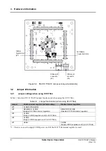
Page 7: ...s J1 J2 J3 and J4 are patterns only and the actual connectors are provided together with the product for mounting as necessary 2 The through hole bore diameter is 0 85 mm Extension Connector J1 foot pattern only 1 2 Reset SW SW1 HVDD IN J7 LVDD IN J8 AVDD IN J9 Extension Connector J2 foot pattern only 1 2 Extension Connector J3 foot pattern only 1 2 Extension Connector J4 foot pattern only 1 2 S1C...

Page 8: ...ble internal regulator default setting Disable internal regulator JP1 CLOSE VIN HVDD JP2 REGEN EN CLOSE Enable S1C17564 internal regulator REGEN DS CLOSE Disable S1C17564 internal regulator JP5 CLOSE Supply AVDD supplied via J9 to S1C17564 JP6 CLOSE Supply HVDD supplied via J7 to S1C17564 JP7 OPEN 1 CLOSE Supply LVDD supplied via J8 to S1C17564 1 There is no need to supply LVDD power via J8 if the...

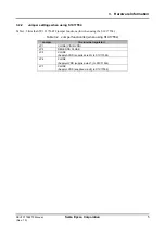
Page 9: ...sts the S5U1C17564T2 jumper functions for when using the S1C17554 Table 3 2 Jumper function list when using S1C17554 Jumper No internal regulator JP1 CLOSE VIN HVDD JP2 REGEN DS CLOSE JP5 CLOSE Supply AVDD supplied via J9 to S1C17554 JP6 CLOSE Supply HVDD supplied via J7 to S1C17554 JP7 CLOSE Supply LVDD supplied via J8 to S1C17554 ...

Page 10: ...3 P20 TOUT2 CAP2 HVDD OSC4 OSC3 VPP OSC2 OSC1 VSS P55 US_SCK1 AIN0 P00 AIN1 P01 AIN2 US_SSI0 P02 AIN3 US_SSI1 P03 AVDD N C TOUT4 CAP4 FOUTA P32 SCL0 P17 VSS HVDD SDA0 P45 EXCL0 SCLK0 TOUT1 CAP1 P42 SOUT0 TOUT7 CAP7 P41 SIN0 TOUT6 CAP6 P40 LVDD RESET C17 0 1uF C16 0 1uF C32 TH only C22 4 7uF C1 1pF C45 0 1uF C29 0 1uF C13 0 1uF R12 33 JP1 FFC 2AMEP1B 1 2 C27 0 1uF C31 10uF R2 10M C7 0 1uF C23 0 1uF...

Page 11: ... 0 1uF C36 0 1uF JP7 FFC 2AMEP1B 1 2 C5 0 1uF R4 10k J7 S2B XH A LF SN 1 2 U2 SN74LVC1G97 1 2 3 6 5 4 In1 GND In0 In2 Vcc Y C11 0 1uF J5 A2 4PA 1 2 3 4 DCLK GND DSIO DST2 U3 S 1000N15 N4T1G 1 2 4 3 OUT VDD GND N C C9 10uF D1 PG1111C JP6 FFC 2AMEP1B 1 2 SW1 SKRAAKE010 C8 10uF J8 S2B XH A LF SN 1 2 J9 S2B XH A LF SN 1 2 J6 S04B PASK 2 1 2 3 4 VPP GND RESET VDD JP5 FFC 2AMEP1B 1 2 C4 0 1uF C43 0 1uF ...

Page 12: ...PASK 2 LF SN 1 JST Mfg Co Ltd Connector J7 J8 J9 S2B XH A LF SN 3 JST Mfg Co Ltd Jumper pin JP1 JP5 JP6 JP7 FFC 2AMEP1B 4 Honda Tsushin Kogyo Co Ltd Jumper pin JP2 WL 1 3P 1 Mac Eight Co Ltd Jumper socket JP1 JP2 JP5 JP6 JP7 5 C1 C2 1 pF 100V 2 C3 C4 C5 C7 C10 C11 C12 C13 C14 C15 C16 C17 C18 C19 C21 C23 C25 C26 C27 C28 C29 C36 C39 C43 C45 0 1 16 V 25 C6 1 6 3 V 1 C20 C22 C24 4 7 6 3 V 3 C8 C9 C31 ...

Page 13: ...Revision History S5U1C17564T2 Manual Seiko Epson Corporation 9 Rev 1 0 Revision History Attachment 1 Code No Page Revision details including previous details and reason 411934300 All New ...

Page 14: ...057 CHINA Phone 86 755 2699 3828 FAX 86 755 2699 3838 EPSON HONG KONG LTD Unit 715 723 7 F Trade Square 681 Cheung Sha Wan Road Kowloon Hong Kong Phone 852 2585 4600 FAX 852 2827 4346 EPSON TAIWAN TECHNOLOGY TRADING LTD 14F No 7 Song Ren Road Taipei 110 TAIWAN Phone 886 2 8786 6688 FAX 886 2 8786 6660 EPSON SINGAPORE PTE LTD 1 HarbourFront Place 03 02 HarbourFront Tower One Singapore 098633 Phone ...

Reviews: