background image

22

  SPECIFICATIONS FOR CPU BOARD CONNECTORS

S5U1C17801T1100 HARDWARE MANUAL


EPSON 

49

(SOFTWARE EVALUATION TOOL FOR S1C17801)

J

13

 Connector

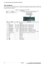
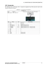
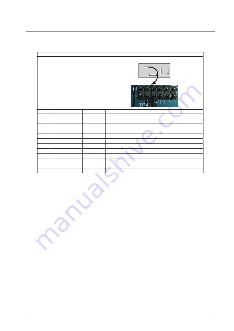
The following shows specifications of J

13

, a connector for expansion board. This connector is used for the 

connection with the LCD board.

Table 

22

.

5

.

1

  J

13

 Connector Pin Assignment

Connector J13

Maker: 

SAMTEC

Model number:  TSW-

106

-

07

-S-D

Front view of CPU board (without LCD panel)

No.

Name

I/O

Functionalities

1

V

DD

Power pin

2

V

DD

Power pin

3

P

33

 (if P

45

=L)

I/O

General purpose I/O port

4

P

34

 (if P

45

=L)

I/O

General purpose I/O port 

5

P

05

/AIN

5

I/O | I

General purpose I/O port  |  Analog input port

6

P

06

/AIN

6

I/O | I

General purpose I/O port  |  Analog input port

7

N.C

8

N.C

9

N.C

10

N.C

11

GND

Power ground

12

GND

Power ground

11

1

12

2

Summary of Contents for S5U1C17801T1100

Page 1: ...CMOS 16 BIT SINGLE CHIP MICROCOMPUTER Software Evaluation Tool for S1C17801 S5U1C17801T1100 Hardware Manual ...

Page 2: ...herwise and there is no representation or warranty that anything made in accordance with this material will be free from any patent or copyright infringement of a third party This material or portions thereof may contain technology or the subject relating to strategic products under the control of the Foreign Exchange and Foreign Trade Law of Japan and may require an export license from the Minist...

Page 3: ... 99 Specs not fixed Specification Package D die form F QFP B BGA Model number Model name C microcomputer digital products Product classification S1 semiconductor Development tools S5U1 C 17000 H2 1 Packing specifications 00 standard packing Version 1 Version 1 Tool type Hx ICE Dx Evaluation board Ex ROM emulation board Mx Emulation memory for external ROM Tx A socket for mounting Cx Compiler packa...

Page 4: ......

Page 5: ...20 8 Jumper Switch Settings 22 Setting for JP1 22 Setting for JP2 23 Setting for JP3 24 9 Connection Circuit to External Memory 25 SRAM Connection Circuit 25 NOR Flash Connection Circuit 26 NAND Flash Connection Circuit 27 EEPROM Connection Circuit 28 10 Power Control Circuit for Battery Backup Function 29 Battery Backup Function 29 Power Control Circuit for Battery Backup Function 29 11 LCD Panel...

Page 6: ... Control of Ports 43 21 Serial 44 22 Specifications For Cpu Board Connectors 45 J6 Connector to Connect with ICD 45 J7 Connector 46 J8 Connector 47 J12 Connector 48 J13 Connector 49 J18 Connector 50 Appendix A How to Measure Current Consumption 51 A 1 Measuring VDD Current Consumption 51 A 2 Measuring AVDD Current Consumption 52 A 3 Measuring RTCVDD Current Consumption 52 ...

Page 7: ...on boards to connect with the SVT17801 CPU Board CPU S1C17801 Input power voltage 5 0V DC Regulator output voltage 3 3V CPU Input Clock OSC1 32 768kHz OSC3 48MHz Built in Functions Devices Reset switch Expansion interface connectors LCD GPIO UART I2C AD ICD board connector SRAM 16Mbit NOR Flash 64Mbit NAND Flash 2Gbit EEPROM 256Kbit Battery backup control circuit Power switch Key input circuit 6 k...

Page 8: ...5U1C17801T1100 package 1 SVT17801 CPU Board Main body 1 2 SVT17801 ICD Board 1 3 SVT17801 LCD Board 1 4 USB Cable 1 5 Coin Battery CR2032 3V 1 6 AC Adapter 1 7 Warranty Registration Card 1 each for English Japanese 8 Warranty Card 1 each for English Japanese 9 Precautions in Use 1 each for English Japanese 10 Manual Download Guide 1 each for English Japanese ...

Page 9: ...of each part Fig 3 1 1 Name of Each Surface Mounted Part with LCD Panel 1 Power LED Blue 7 LED 13 Key switch 2 Speaker Left 8 POWER SW 14 Crystal oscillator 48MHz 32KHz 3 RESET SW 9 GND pin 15 S1C17801 4 USBminiB connector 10 Speaker Right 16 LCD board 5 LED RGB 11 JP pin 6 MIC 12 Expansion connector 2 1 3 4 5 6 7 8 9 13 15 3 5inch STN QVGA B W Membrane touch panel 14 9 16 9 CPU board ICD board 10...

Page 10: ...7801T1100 HARDWARE MANUAL SOFTWARE EVALUATION TOOL FOR S1C17801 Fig 3 1 2 Name of Each Surface Mounted Part without LCD Panel 1 Infrared emitting module LED 3 SRAM 5 Expansion connector LCD board 2 FLASH NOR 4 FLASH NAND 1 2 5 CPU board ICD board 3 4 ...

Page 11: ...SW 8 Power supply connector 5V 15 USBminiB connector 3 ICDminiI F 9 AudioCodec 16 Bus connector Not available 4 ICD board connector 10 Power Switch 17 Coin Battery 5 Placement of infrared receiver module substitute 11 AudioCodec Oscillator 18 Measuring JP for IC consumed current 12 MMC Card Socket 6 Audio connector OUT 13 Infrared receiver module 19 EEPROM CPU board ICD board 4 1 2 3 5 6 7 19 18 1...

Page 12: ...OF EACH PART 6 EPSON S5U1C17801T1100 HARDWARE MANUAL SOFTWARE EVALUATION TOOL FOR S1C17801 Fig 3 1 4 Name of Each Part Mounted on Rear Face of LCD Board 1 Connector to connect LCD panel 2 Connector to connect CPU board 1 2 ...

Page 13: ...112 20 46 137 102 25 167 2 55 Parts installed within this dash line must be max 8 mm in height 100 89 5 5 80 7 90 50 22 10 9 φ3 3 hole 9 φ7 10 9 1 D1 Installation instruction diagram Rear Face J11 J9 J6 U23 1 3 J15 J14 6 4 4 4 50 52 5 140 155 185 110 72 5 37 5 15 2 67 5 55 10 5 8 2 9 φ7 SW1 3 32 912345678 J5 80 110 155 CARD CENTR 4 J10 1 5 1 BAT1 3 1 2 J4 1 2 3 1 4 2 3 U21 1 3 1 5 2 10 1 9 1 4 1 4...

Page 14: ...d Dimensions The following drawing shows dimensions of the ICD board Parts Side View 4 21 5 37 5 43 50 4 φ3 5 through hole 4 R 2 4 4 φ7 land 5 5 9 JUSB 1 5 Soldering Side View 4 95 JICD 1 2 9 10 Fig 3 2 2 1 ICD Board Dimensions Precautions Unit for the above dimensions is millimeter mm Material FR4 Board thickness 1 6 mm ...

Page 15: ... 6 φ3 3 NTH 19 5 15 10 5 3 5 5 80 10 51 51 20 90 65 5 Rear Face View from Surface 6 φ7 6 φ3 3 hole 102 26 29 Hole 19 20 5 51 51 112 J101 J103 J102 J104 17 11 14 1 12 1 1 4 2 18 1 2 3 70 5 65 5 80 5 10 55 90 50 50 20 10 15 Fig 3 2 3 1 LCD Board Dimensions Precautions Unit for the above dimensions is millimeter mm Board thickness 1 6 mm Figure 3 2 3 1 is a rear face drawing seen from the board surfa...

Page 16: ...viewing area of touch panel 58 59 0 3 viewing area of bazel 58 active area of touch panel 57 59 0 01 display area 4 4 7 5 0 5 205 9 3 Max 7 1 13 P1 0 13 W 0 7 VIEWING DIRECTION BOTTOM 0 6 6 2 PIN1 IF2 60 9 RIGHT LEFT 10 2 STIFFER 7 1 STIFFER CONTACT SIDE A 6 3 30 0 7 3 7 9 8 405 0 3 0 05 CONTACT SIDE 2 R0 3 4 0 0 3 UNIT mm SCALE NTS NOT SPECIFIED TOLERANCE IS 0 5 CONDUCTOR A DETAIL 5 0 1 1 0 1 0 3...

Page 17: ...Infrared emitting module D1 AN333 STANLEY Infrared receiver module U21 GP1UX311QS SHARP Infrared receiver module for U21 PNA4702M Panasonic AudioCodec U22 PCM3793ARHB TI AudioCodec Oscillator OSC1 SG 8002JC 12 288M PCCB EPSON TOYOCOM CORP Audio connector J14 SJ 43514 SMT CUI Inc Audio connector J15 SJ 3523 SMT CUI Inc Speakers SP1 SP2 NDT 03B STAR MICRONICS MIC MIC1 EM6022P 42BC10 33 G Horn Indust...

Page 18: ...sically the communication connection becomes in the stand by status ICD Board LED The LED indicates ICD board and target statuses in different colors Blue Power on before the initial connection with the target is established Green The target is currently in debug mode Red The target is not connected or not properly connected The target is currently executing a user program CPU Board The CPU board ...

Page 19: ... Step 2 Figure 3 4 2 2 shows the installation has been completed Fig 3 4 2 2 Installing Removing Coin Battery 2 4 Remove Step 1 Insert a slotted screw driver into space between the coin cell and socket lift the driver up as a lever and move it in the direction of arrow to secure a small space on the right side of the socket as shown in the figure 3 4 2 3 Fig 3 4 2 3 Installing Removing Coin Batter...

Page 20: ...niB USB 2 0 FS I2C SW 5V DC 100V AC Regul ator 5V 3 3V SRAM FLASH ADx ADx EPPROM Card i f GPIO RTC RAM UART NAND FLASH Audio input MFT0 SW LED ADx ADx ADx ICD connector ADx GPIO Speaker I O connector ICD mini connector ICDmini External Device Coin Cell ADx GPIO Audio jack Microphone Bus Audio jack Infrared LED Rotary switch Receiving module Touch panel control Bus connector Not available LCD panel...

Page 21: ...ironments the target CPU the S1C17801 on the CPU board operates according to commands executed by a debugger on your PC connected with the ICD board A command executed by the debugger is sent to the ICD board via USB to be analyzed and converted into a debug signal and then sent to the CPU board The debugger on your PC can be used to download programs or data to the CPU board or debug programs by ...

Page 22: ...at LED on the ICD board lights in blue green the target is in debug mode 6 Start the debugger on your PC to execute the program Make sure that LED on the ICD board lights in red the target is in normal mode For details on the operation of the debugger and debugging commands see the S5U1C17001C Manual S1C17 Family C Compiler Package Note Be sure never to disconnect a USB cable between PC and ICD bo...

Page 23: ... HARDWARE MANUAL EPSON 17 SOFTWARE EVALUATION TOOL FOR S1C17801 When the USB driver has been installed successfully it appears on the device manager as shown below Notes If the driver does not appears on the device manager as shown above install the USB driver again ...

Page 24: ...1 For information about downloading a program see the S5U1C17001C Manual S1C17 Family C Compiler Package 4 After exiting the debugger remove the USB cable to disconnect the ICD board from your PC 5 Disconnect the ICD board from the CPU board and install a coin cell battery 6 Press the reset switch on the CPU board Then the S1C17801 on the CPU board starts executing a user pro gram downloaded to th...

Page 25: ...d of data download Approx 65KB s DCLK at 40MHz Max 1 Approx 50KB s DCLK at 20MHz 1 4 Communications frequency with target DCLK frequency 4KHz 40MHz Standalone flash writer function Available None Firmware update function Available Power supply for writing to flash ROM Available None Reset signal output to target Available Target system I O support voltage 3 3V 1 8V and voltage input from target 1 ...

Page 26: ...decIC TP48 P26 I O I2S1 P26 I2S_SCK1 AudioCodecIC TP47 P27 I O I2S1 P27 I2S_MCLK1 AudioCodecIC TP51 P30 I O TM0 P30 TM0 Switch IC Uni color LED P31 I O TM0 ADTRG P31 TM0 ADTRG Rotary encoder key input P32 I O WDT CMU P32 WDT_CLK WDT_NMI CMU_CLK Switch IC P33 I O Memory TM0 P33 SMRD TM0 Switch IC NAND Flash or expansion I F Connector No J13 P34 I O Memory P34 SMWR P35 I O ICD i f P35 DCLK ICD I F C...

Page 27: ...ash NAND Flash P91 I O Memory P91 D1 P92 I O Memory P92 D2 P93 I O Memory P93 D3 P94 I O Memory P94 D4 P95 I O Memory P95 D5 P96 I O Memory P96 D6 P97 I O Memory P97 D7 PA0 I O Memory PA0 CE0 NOR Flash PA1 I O Memory PA1 CE1 SRAM PA2 I O Memory PA2 CE2 NAND Flash PA3 I O Memory PA3 CE3 NAND Flash PA4 I O Memory PA4 RD NOR Flash SRAM PA5 I O Memory PA5 WRL NOR Flash SRAM PA6 I O Memory PA6 WRH BSH ...

Page 28: ...ng 1 2 on JP1 must be shorted to select Wakeup Enable Wakeup Enable can be controlled by the Wakeup pin on the S1C17801 or on board power switch For details see the description of RTC control circuit in Chapter 10 Shorting 2 3 on JP1 disables the Wakeup func tion Factory default setting for JP1 is Wakeup Enable To 3 3V regulator JP1 JP1 JP1 ENABLE WAKEUP DISABLE WAKEUP To POWER SW To WAKEUP pin 1 ...

Page 29: ...t 2 3 on JP2 to se lect VDD for the power supply to RTCVDD whereas 1 3 to select battery For details see the description of RTC control circuit in Chapter 10 Note that when 1 2 is shorted a coin cell battery is required to activate RTCVDD Factory default setting for JP2 is 1 2 shorted JP2 JP2 C55 0 1µF C47 10µF JP2 DIC 149 3P 1 2 1 2 3 To RTCVDD VDD D10 CRS06 BAT1 106 V DD Battery Fig 8 2 1 JP2 Re...

Page 30: ... of LCD backlight Shorting 1 2 is not allowed while 2 3 is shorted For details see Chapter 15 LED LCD BACKLIGHT CONTROL CIRCUIT WITH MFT0 5 6 Shorted Power with phase generated by MFT0 is supplied to LED3 It can be used to adjust the brightness of LED3 Ei ther 1 2 or 2 3 can be shorted while 5 6 is shorted For details see Chapter 15 LED LCD BACKLIGHT CON TROL CIRCUIT WITH MFT0 Factory default sett...

Page 31: ... SVT17801 VDD VDD A0 A1 A2 A3 A4 A5 A6 A7 A8 A9 A10 A11 A12 A13 A14 A15 A16 A17 A18 A19 A1 A2 A3 A4 A5 A6 A7 A8 A9 A10 A11 A12 A13 A14 A15 A16 A17 A18 A19 A20 D0 D1 D2 D3 D4 D5 D6 D7 D8 D9 D10 D11 D12 D13 D14 D15 A 20 D0 D1 D2 D3 D4 D5 D6 D7 D8 D9 D10 D11 D12 D13 D14 D15 CY62167DV30 S1C17801 NC DNU VCC 29 31 33 35 38 40 42 44 30 32 34 36 39 41 43 45 VSS VSS CE1 RD WRL WRH RSH A0 BSL 25 24 23 22 21...

Page 32: ... A14 A15 A16 A17 A18 A19 A20 A21 A1 A2 A3 A4 A5 A6 A7 A8 A9 A10 A11 A12 A13 A14 A15 A16 A17 A18 A19 A20 A21 A22 D0 D1 D2 D3 D4 D5 D6 D7 D8 D9 D10 D11 D12 D13 D14 D15 A 1 D0 D1 D2 D3 D4 D5 D6 D7 D8 D9 D10 D11 D12 D13 D14 D15 S29JL064H S1C17801 VCC 29 31 33 35 38 40 42 44 30 32 34 36 39 41 43 45 VSS VSS CE0 RD WRL P44 RESET 25 24 23 22 21 20 19 18 8 7 6 5 4 3 2 1 48 17 16 9 10 13 A1 to A22 D0 to D15...

Page 33: ...to the SVT17801 VDD VDD D0 D1 D2 D3 D4 D5 D6 D7 NC NC NC NC NC NC NC NC NC NC NC NC NC NC D0 D1 D2 D3 D4 D5 D6 D7 MT29F2G08AACWP S1C17801 29 30 31 32 41 42 43 44 25 26 27 28 33 34 35 38 39 40 45 46 47 48 VCC VCC VSS VSS CE2 SMRD SMWR 1 2 3 4 5 6 10 11 14 15 20 21 22 23 24 D0 to D7 R B WP CE RE WE CLE ALE 37 12 36 13 10K 10K R87 R82 R74 10K 10K R89 R88 10K NC NC NC NC NC NC NC NC NC NC NC NC NC NC ...

Page 34: ...801 EEPROM Connection Circuit MICROCHIP 256K bits EEPROM 24AA256 is installed on the SVT17801 The following diagram shows how the EEPROM is connected to the SVT17801 1 5 6 SCL WC VCC VSS SDA E0 E1 E2 3 8 7 4 2 VDD S1C17801 U17 24AA256 I SN I2C_SDA R5 2 2K R6 2 2K I2C_SCL C9 0 1µF Fig 9 4 1 EEPROM connection circuit ...

Page 35: ...t operating RTC and retaining contents inside IVRAM with low power consumption Because the power is supplied only to the minimum indispensable functions leak current can also be reduced drastically compared with sleep mode AVDD VDD RTCVDD S1C17801 The SVT17801 is designed to connect the coin battery CR2032 with RTCVDD enabling RTC to keep functioning and IRAM to retain its contents even if power s...

Page 36: ...y respectively both factory default JP2 is located just before the WAKEUP pinʼs entering into an OR circuit and if JP2 is set to WAKEUP DIS ABLE 5V instead of WAKEUP pin is input to the OR circuit turning regulator always ON JP3 selects supply source of RTCVDD shown in the figure 10 2 1 If Battery is selected RTCVDD is supplied from the coin cell battery CR2032 and if VDD is selected RTCVDD is sup...

Page 37: ...ile the power switch is being pressed the output of regulator shown in figure 10 2 1 becomes 3 3V S1C17801 starts operating and immediately after that the standby mode is released by turning the WAKEUP signal HIGH By turning the WAKEUP signal HIGH at Step the output of regulator shown in figure 10 2 1 be comes always 3 3V This power control circuit should be used only for reference The circuit is ...

Page 38: ...S61040 L101 LQH32CN4R7M23L L102 MPZ2012S601A VDD D101 B0530W 7 F 1 SW FB GND VIN EN 3 2 4 5 C105 22PF Q105 MMBTA42 TP Fig 11 1 LCD Panel Module Connection Circuit This panel module is equipped with a 4 bit STN LCD panel to which data bus is connected as shown above The following lists function of each signal on the module side Table 11 1 Name and Function of Signal on LCD Panel Module Signal Name ...

Page 39: ...AIN6 0 to VDD V LOW LCD panel module LEFT HIGH Hi Z TOP Hi Z HIGH RIGHT LOW 0 to VDD V BOTTOM 0 to VDD V LOW In order to obtain panelʼs touch position information on X axis of the figure 11 1 2 an AD value obtained from AIN6 is used to determine the position of X axis when P33 is turned LOW while P34 HIGH as shown in X axis fields shown in the table 11 1 1 The AIN6 value becomes gradually larger f...

Page 40: ...s shown in the figure 12 1 If any of the switches is pressed on the other hand the pull down resistor value becomes smaller than the pull up resistor value and this turns the port P31 LOW The mechanism of this circuit enables the press of any switch to be detected by using interrupt or other method Figure 12 1 also indicates that the pressed switch can be determined by the variance of ratio betwee...

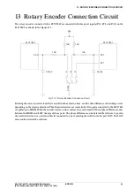
Page 41: ...ion Circuit Rotating the rotary encoder closes the A and B switches shown above and the time difference of switching occurs depending on the rotative direction When the encoder does not rotate both of two ports connected to the S1C17801 are pulled up to HIGH When the encoder rotates on the contrary they are turned LOW and phase difference arises between the HIGH and LOW timings of those ports The ...

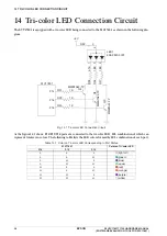
Page 42: ... MMBTA42 TP Q4 Q2 Q3 1K R29 1K R30 1K R28 R26 R27 5 1K 1 8K 1 8K 1 2 3 0 4 Fig 14 1 Tri color LED Connection Circuit As the figure 14 1 shows P14 P15 P16 ports are connected to the tri color LED H L combination of which can represent total seven colors The following table lists the LED colors formed by H L combination of each port Table 14 1 Color on Tri color LED Corresponding to Port Status S1C1...

Page 43: ...66 R90 470 LED3 LTW 170TK C65 0 1µF LCD_BL_ON LCD_BL_PWM D201_PWM S1C17801 Fig 15 1 Connection Circuit between MFT0 and LED LCD Backlight Pre stage switching IC TS5A3166 is switched by changing phase in MFT0 H L areas and brightness of the LED can be changed visually by turning ON and OFF the backlight of LED and LCD panel repeatedly in accordance with the MFT0 phase MFT0 is an I O port with 12 mA...

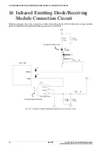
Page 44: ...Following diagram shows the connection of infrared emitting diode AN333 infrared receiving modules GP1UX31QS GP1UX51QS PNA4702M installed on the SVT17801 VDD VDD C15 4 7µF C66 10µF C14 4 7µF R12 100 D1 AN333 S1C17801 REMO VOUT GND VCC REMI U21 1 2 3 GP1UX311QS Q1 MMBTA42 TP R14 1K R24 47 Infrared Emitting Diode Infrared Receiver Module Fig 16 1 Infrared Emitting Diode Receiving Module Connection C...

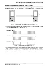
Page 45: ...cribes the transmit waveform from REMO on the S1C17801 and corresponding waveforms and For the monitoring points of to see Table 16 1 Waveform for Waveform for Waveform for Fig 16 1 2 Waveform for Each Point Shown in Figure 16 1 Infrared communication in this case covers approximately 3 m by our measurement when emitting and receiving modules are placed face to face without any obstacle between th...

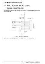
Page 46: ...e SVT17801 is equipped with a MMC card socket being connected to the S1C17801 with SPI mode as shown in the following diagram VDD J5 DM1B DSF PEJ 22 R17 10K R18 10K R16 10K C16 0 1µF 1 2 3 4 5 6 7 8 9 SPI_SSI0 SPI_SDO0 SPI_SCK0 SPI_SDI0 MMC_CARD Fig 17 1 MMC Card Connection Circuit For information about controlling the MMC card using SPI mode see the Application Note ...

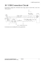
Page 47: ... S1C17801 as shown in the following diagram VDD S1C17801 D4 1N5819 D6 1N5819 C21 1µF L5 BLM21PG600SN1D R25 R52 R22 R23 1 5K 5 1K 22 22 U19 SN65220DBVT A GND B NC GND NC J10 54819 0578 1 2 3 4 5 FG6 FG7 FG8 FG9 VBUS D D ID GND 6 5 4 1 2 3 USB C24 22P C51 22P PUENB USBVBUS USBDM USBDP R53 10K D3 1N5819 D5 1N5819 Fig 18 1 USB Connection Circuit For information about controlling USB see the Applicatio...

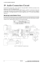
Page 48: ...ection Status P32 SCKI PCM3793 status H Connects to SG 8002JC 12 288MHz crystal L Connects to I2S_MCLKO VDD VDD OSC1 SG 8002JC 12 288M U32 TS5A3159A G V VDD R55 33 R83 47K 2 OE GND VDD OUT 3 4 4 1 6 3 2 5 L6 L7 BLM18PG300SN1D BLM18PG300SN1D C41 10µF AVDD R54 10K R46 10K S1C17801 S1C17801 I2C SCL I2C_SDA I2S MCLK1 I2S SDI1 I2S_SDO0 I2S_WS0 1 I2S_SCK0 1 I2S_MCLK0 P32 C43 C44 C45 C53 0 1µF 4 7µF 4 7µ...

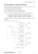
Page 49: ...5 Status and Connection Status of PC3 PC2 P34 P33 and PA2 P45 PC3 PC2 P34 P33 PA2 H NAND Flash NAND Flash NAND Flash NAND Flash NAND Flash L J8 connector Power switch LCD module LCD module J8 connector Note that the P45 port becomes an input port immediately after reset has been released In this status P45 is pulled down to LOW The following diagram shows a circuit in this area VDD C50 0 1µF R67 1...

Page 50: ...d to Multiplex SPI ch0 SD I F through holes TP52 TP53 TP54 TP55 SPI GPIO P10 P11 P12 P13 SPI ch1 Tri color LED SPI GPIO P13 P14 P15 P16 UART Expansion I F J8 through holes TP42 TP43 TP44 UART GPIO P40 P41 P42 I2C Expansion I F J8 EEPROM AudioCodec I2C GPIO P50 P51 I2S ch0 AudioCodec through holes TP47 TP48 TP49 TP50 TP51 SPI GPIO P20 P21 P22 P23 I2S ch1 AudioCodec through holes TP47 TP48 TP49 TP50...

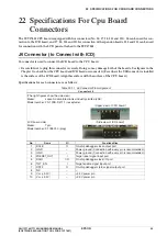
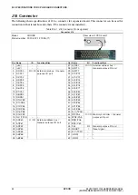
Page 51: ...where the USB connector is installed is the surface of the ICD board Align this surface with the surface of the CPU board Specifications for each connector are as follows Table 22 1 1 J6 Connector Pin Assignment Connector J6 The right figures show the side view Maker Japan Aviation Electronics Industry Limited JAE Model number PS 10SD D4T1 1 receptacle Upper view of CPU board ICD board side Maker ...

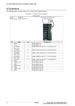
Page 52: ... AVDD Analog power pin 3 P00 AIN0 I I General purpose input port Analog input port 4 N C TP9 5 P01 AIN1 I I General purpose input port Analog input port 6 N C TP10 7 P02 AIN2 I I General purpose input port Analog input port 8 N C TP11 9 P03 AIN3 I I General purpose input port Analog input port 10 N C TP12 11 P04 AIN4 I I General purpose input port Analog input port 12 GND Analog power ground 13 GN...

Page 53: ...ies 1 VDD Power pin 2 VDD Power pin 3 P50 I2C_SDA I O I O General purpose I O port I2C data I O pin 4 N C TP22 5 P51 I2C_SCL I O I O General purpose I O port I2C clock I O pin 6 N C TP23 7 PC3 if P45 L I O General purpose I O port 8 N C TP24 9 PA2 if P45 L I O General purpose I O port 10 N C TP31 11 P40 SIN0 TP42 I O I General purpose I O port UART data input pin 12 N C TP32 13 P41 SOUT0 TP43 I O ...

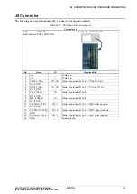
Page 54: ...urpose I O port Display data bus 4 PC5 FPDAT5 I O O I O General purpose I O port Display data bus 5 PC6 FPDAT6 I O O I O General purpose I O port Display data bus 6 PC7 FPDAT7 I O O I O General purpose I O port Display data bus 7 P54 FPFRAME I O O General purpose I O port Frame clock 8 P55 FPLINE I O O General purpose I O port Display data line clock 9 P56 FPSHIFT I O O General purpose I O port Di...

Page 55: ...e 22 5 1 J13 Connector Pin Assignment Connector J13 Maker SAMTEC Model number TSW 106 07 S D Front view of CPU board without LCD panel No Name I O Functionalities 1 VDD Power pin 2 VDD Power pin 3 P33 if P45 L I O General purpose I O port 4 P34 if P45 L I O General purpose I O port 5 P05 AIN5 I O I General purpose I O port Analog input port 6 P06 AIN6 I O I General purpose I O port Analog input po...

Page 56: ... bus General purpose I O port 2 5V 28 A8 P70 3 D0 P90 I O I O External data bus General purpose I O port 29 A9 P71 4 D1 P91 30 A10 P72 5 D2 P92 31 A11 P73 6 D3 P93 32 A12 P74 7 D4 P94 33 A13 P75 8 D5 P95 34 A14 P76 9 D6 P96 35 A15 P77 10 D7 P97 36 A16 P80 11 D8 PB0 37 A17 P81 12 D9 PB1 38 A18 P82 13 D10 PB2 39 A19 P83 14 D11 PB3 40 A20 P84 15 D12 PB4 41 A21 P85 16 D13 PB5 42 A22 P86 17 D14 PB6 43 ...

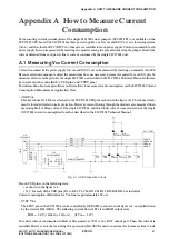
Page 57: ...easurement Application Note USB Pins Shot key diodes D3 to D6 are attached to the SVT17801 USB pins as shown in the figure A 1 The diodes attach ment is intended for electrostatic protection However current flowing through the diodes is also measured when measuring Halt or Sleep current of the single S1C17801 and this diodes current causes deviation of the single S1C17801 current consumption from ...

Page 58: ...5 Note that sample software software flow for measuring the current consumption the software referred in the S1C17801 Current Consumption Measurement Application Note does not control the AVDD line A 3 Measuring RTCVDD Current Consumption Current consumed by the power supply for IVRAM and RTC inside battery backup area RTCVDD can be measured by inserting an ammeter into JP2 When JP2 is measured be...

Page 59: ...i Hong Kong Phone 852 2585 4600 Fax 852 2827 4346 Telex 65542 EPSCO HX EPSON CHINA CO LTD SHENZHEN BRANCH 12 F Dawning Mansion Keji South 12th Road Hi Tech Park Shenzhen Phone 86 755 2699 3828 Fax 86 755 2699 3838 EPSON TAIWAN TECHNOLOGY TRADING LTD 14F No 7 Song Ren Road Taipei 110 Phone 886 2 8786 6688 Fax 886 2 8786 6660 EPSON SINGAPORE PTE LTD 1 HarbourFront Place 03 02 HarbourFront Tower One ...

Page 60: ...008 Printed in Japan A H Software Evaluation Tool for S1C17801 S5U1C17801T1100 Hardware Manual EPSON Electronic Devices Website SEMICONDUCTOR OPERATIONS DIVISION http www epson jp device semicon_e Document code 411524500 ...

Reviews: