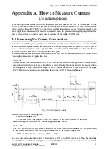
Appendix A HOW TO MEASURE CURRENT CONSUMPTION
S5U1C17801T1100 HARDWARE MANUAL
EPSON
51
(SOFTWARE EVALUATION TOOL FOR S1C17801)
Appendix A How to Measure Current
Consumption
For measuring current consumption of the single S
1
C
17801
unit, jumpers (JP
4
,JP
5
,JP
2
) are available on the
SVT
17801
CPU board. The S
1
C
17801
has three power supplies, one for core and I/O (V
DD
), one for analog system
(AV
DD
), and the other for RTC (RTCV
DD
). Jumpers are available for each power supply. Current consumed by each
power supply line can be measured by inserting an ammeter among the pins after removing the jumper. Sum of the
current obtained from each power line is current consumed by the single S
1
C
17801
unit.
A.
1
Measuring V
DD
Current Consumption
Current consumed by the power supply for core and I/O (V
DD
) can be measured by inserting an ammeter into JP
4
.
Because external components affect the measurement, some necessary process is required for each I/O pin. To
measure current consumption for the single S
1
C
17801
as described in the S
1
C
17801
Technical Manual, influence
by current must be controlled for "USB pins" and "STBY pins."
For information about sample software (software flow) to measure current consumption, see the S
1
C
17801
Current
Consumption Measurement Application Note.
∗
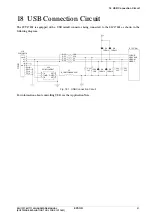
USB Pins
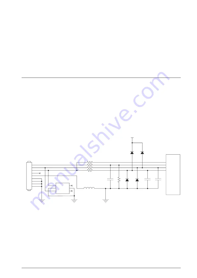
Shot key diodes D
3
to D
6
are attached to the SVT
17801
USB pins as shown in the figure A.
1
. The diodes attach-
ment is intended for electrostatic protection. However, current flowing through the diodes is also measured when
measuring Halt or Sleep current of the single S
1
C
17801
, and this diodes current causes deviation of the single
S
1
C
17801
current consumption from that described in the S
1
C
17801
Technical Manual.
J10
54819-0578
1
2
3
4
5
FG6
FG7
FG8
FG9
6
5
4
1
2
3
USB
U19
SN65220DBVT
L5
BLM21PG600SN1D
R25
R52
R22
R23
1.5K
5.1K
22
22
VBUS
D–
D+
ID
GND
A
GND
B
NC
GND
N
C21
1µF
C24
22P
C51
22P
PUENB
S1C17801
USBVBUS
USBDM
USBDP
R53
10K
D3
1N5819
D4
1N5819
V
DD
D6
1N5819
D5
1N5819
Fig. A.
1
USB Connection Circuit
If each USB pin is in the following state,
• as shown in the figure A.
1
.,
• N.C. for each of the USB pins (D
3
to D
6
, C
51
,C
24
,R
53
,C
21
,R
25
,R
52
,R
22
,R
23
not installed)
Current consumption differential for V
DD
line is approximately
100
μ
A.
∗
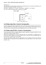
STBY Pins
The STBY pin on the SVT
17801
can be controlled by GPIO(P
43
) as shown in the figure A.
2
, and pulled down
by the resistor R
21
(
10
K
Ω
). The following current flows if P
43
is in HIGH output state.
IR
21
=
3
.
3
(V) /
10
(k
Ω
) =
330
(
μ
A)
(if V
DD
=
3
.
3
V)
To reduce current consumption in Halt or Sleep mode, set P
43
to the LOW output port. Then this current is
cancelled. However, note that executing this operation while OSCI is used as a system clock causes system to halt
Summary of Contents for S5U1C17801T1100
Page 4: ......


