GRAPHICS
SED1352
X16B-C-001-06
15
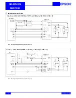
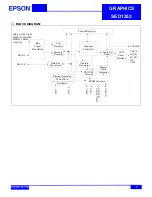
Display Memory Interface
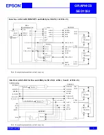
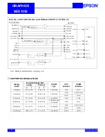
LCD Interface
a
VESA Flat Panel Display Interface Standard (FPDI-1
TM
)
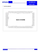
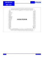
Pin Name Type F0B Pin #
F1B Pin #
D0B Pad
#
Description
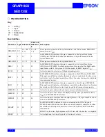
VD0-VD15 I/O
44 - 51,
54 - 61
41 - 48,
51 - 58
These pins are connected to the display memory data bus. For 16-bit interface,
VD0-VD7 are connected to the display memory data bus of even byte addresses
and VD8-VD15 are connected to the display memory data bus of odd byte
addresses. The output drivers of these pins are tri-stated when RESET is high.
On the falling edge of RESET the values of VD0-VD15 are latched into the chip to
configure various hardware options.
VD0-VD15 each have an internal pull-down resistor
VA0-VA15 O
33 - 43,
62 - 66
30 - 40
59, 63
These pins are connected to the display memory address bus.
VCS1#
O
69
66
Active low chip-select output to the second or odd byte address SRAM.
VCS0#
O
68
65
Active low chip-select output to the first or even byte address SRAM.
VWE#
O
67
64
Active low output used for writing data to the display memory. This pin is
connected to the WE# input of the SRAMs.
VOE#
O
83
80
Active low output to enable reading of data from the display memory. This pin is
connected to the OE# input of the SRAMs.
Pin Name
FPDI-1
TM
Pin Name
a
Type F0B Pin #
F1B Pin #
D0B Pad #
Description
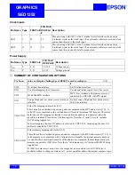
UD3-UD0
UD3-UD0
O
70 - 73
67 - 70
Upper panel display data for dual panel mode. For single panel
mode, these bits are the most significant 4 bits of the 8 bits output
data to the panel (PD[4:7]). For 4-bit single panel mode, these bits
are the 4 bits of output data to the panel.
LD3-LD0
LD3-LD0
O
74 - 77
71 - 74
Lower panel display data for dual panel mode. For 8-bit single panel
mode, these bits are the least significant 4 bits of the 8 bits output
data to the panel (PD[0:3]). For 4-bit single panels, these bits are
driven 0 (low state).
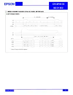
XSCL
FPSHIFT
O
81
78
Display data shift clock. Data is shifted into the LCD X-drivers on
the falling edge of this signal.
LP
FPLINE
O
79
76
Display data latch clock. The falling edge of this signal is used to
latch a row of display data in the LCD X-drivers and to turn on the
row driver (Y driver).
WF
MOD
O
80
77
LCD backplane BIAS signal. This output toggles once every n LP
periods, as programmed in AUX[5]
YD
FPFRAME O
78
75
Vertical scanning start pulse. A logic ‘1’ on this signal, sampled by
the LCD module on the falling edge of LP, is used by the panel row
driver (Y driver) to indicate the start of the vertical frame.
LCDENB
O
82
79
LCD enable signal output. It can be used externally to turn off the
panel supply voltage and backlight.

