Epson Research and Development
Page 47
Vancouver Design Center
Hardware Functional Specification
SED1352
Issue Date: 99/07/28
X16-SP-001-16
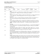
bit 7
DISP
This bit selects display on or off. When this bit = 0, Display OFF is selected (LD0-3 and UD0-3 are forced
to 0). When this bit = 1, Display ON is selected. This bit goes low on RESET.
bit 6
Panel
This bit selects the LCD panel configuration (single or dual). When this bit = 0, Single LCD panel drive is
selected. When this bit = 1 Dual LCD panel drive is selected. This bit goes low on RESET.
bit 5
Mask XSCL
When this bit = 0 XSCL is not masked off during the horizontal non-display period. When this bit = 1
XSCL is masked off during the horizontal non-display period. This bit goes low on RESET.
bit 4
LCDE
The state of this pin determines the state of output pin 82, LCDENB, and is intended for control of an
external LCDBIAS power supply. However, this pin can be used as a General I/O pin if desired. When
LCDE = 0, LCDENB is forced low. When LCDE = 1, LCDENB is forced high. This bit goes low on
RESET.
bit 3
Gray Scale
Selects between 16-level or 4-level gray scale display. When this bit = 1, 16 gray shades are displayed (4
bits/pixel). When this bit = 0, 4 gray shades are displayed (2 bits/pixel). This bit goes low on RESET.
bit 2
LCD Data Width
Selects between 4-bit and 8-bit display data widths for single LCD mode. When this bit = 1, 8-bit data
transfer width is enabled. When this bit = 0, 4-bit data transfer width is enabled. In dual panel mode the
data transfer width is forced to 4 bits per panel. This bit goes low on RESET.
bit 1
Memory Interface
This bit selects between the 8-bit or 16-bit memory interface. When this bit = 0, the 16-bit memory inter-
face is selected. When this bit = 1, the 8-bit memory interface is selected. If 16-bit bus interface is selected
(VD0 = 1 on RESET), the Memory Interface bit is forced to 0 internally (16-bit). This bit goes low on
RESET.
bit 0
RAMS
This bit configures the display memory address lines for an 8-bit memory interface system. When this bit
= 0, addressing for 8Kx8 SRAM on an 8-bit display memory data bus interface is selected. When this bit =
1, addressing for 32Kx8 SRAM on an 8-bit display memory data bus interface is selected. This bit goes
low on RESET. This bit is ignored for a 16-bit memory interface.
AUX[01h] Mode Register
I/O address = 0001b, Read/Write.
DISP
Panel
Mask
XSCL
LCDE
Gray Scale
LCD Data
Width
Memory
Interface
RAMS


