background image

SED1352 Dot Matrix Graphics LCD Controller

Programming Notes and Examples

Document Number: X16-BG-007-04

Copyright © 1996, 1998 Epson Research and Development, Inc. All Rights Reserved.

Information in this document is subject to change without notice. You may download and use this document, but only for your own use in
evaluating Seiko Epson/EPSON products. You may not modify the document. Epson Research and Development, Inc. disclaims any

representation that the contents of this document are accurate or current. The Programs/Technologies described in this document may contain 

material protected under U.S. and/or International Patent laws.
EPSON is a registered trademark of Seiko Epson Corporation. All other trademarks are the property of their respective owners.

Summary of Contents for SED1352

Page 1: ...t only for your ownuse in evaluating Seiko Epson EPSON products You may not modify the document Epson Research and Development Inc disclaims any representation that the contents of this document are accurate or current The Programs Technologies described in this document may contain material protected under U S and or International Patent laws EPSON is a registered trademark of Seiko Epson Corpora...

Page 2: ...Page ii Epson Research and Development Vancouver Design Center SED1352 Issue Date 98 10 08 THIS PAGE LEFT BLANK ...

Page 3: ...rograms contact Application Engineering Support Application Engineering Support Engineering and Sales Support is provided by Japan Seiko Epson Corporation Electronic Devices Marketing Division 421 8 Hino Hino shi Tokyo 191 8501 Japan Tel 042 587 5812 Fax 042 587 5564 http www epson co jp Hong Kong Epson Hong Kong Ltd 20 F Harbour Centre 25 Harbour Road Wanchai Hong Kong Tel 2585 4600 Fax 2827 4346...

Page 4: ...Page iv Epson Research and Development Vancouver Design Center SED1352 Issue Date 98 10 08 THIS PAGE LEFT BLANK ...

Page 5: ...R S REFERENCE SED1352 Programming Notes and Examples UTILITIES 1352SHOW EXE Display Utility VIRTUAL EXE Display Utility BIOS1352 COM Utility 1352GRAY EXE Display Utility 1352PD EXE Power Down Utility 1352READ EXE Diagnostic Utility EVALUATION SDU1352B0C Rev 1 0 Evaluation Board User Manual APPLICATION NOTES Power Consumption ISA Bus Interface Considerations MC68340 Interface Considerations LCD Pan...

Page 6: ...Page vi Epson Research and Development Vancouver Design Center SED1352 Issue Date 98 10 08 THIS PAGE LEFT BLANK ...

Page 7: ...DY or WAIT signal option to use built in index register or direct mapping to access one of fifteen internal registers 2 terminal crystal input for internal or external crystal oscillator 8 16 bit SRAM interface configurations two software power save modes low power consumption display modes 2 bit pixel 4 level gray scale display 4 bit pixel 16 level gray scale display virtual display support displ...

Page 8: ...DY A20 to A23 AB0 LDS Decoder A16 A14 A10 to A19 FC0 to FC1 Interface with 16 Bit MC68xxx MPU and 16Kbytes SRAM 2 of 8K x 8 64 Kbit VWE VD0 7 VCS0 VCS1 VA0 12 WE CS 64 Kbit WE CS VD8 15 MEMCS MEMW MEMR READY DB0 to DB7 AB0 to AB15 IOCS IOW IOR RESET SED1352 Z80 RESET D0 to D7 WAIT A0 to A15 WR RD Decoder IORQ A10 to A15 Decoder MREQ Interface with 8 Bit Z80 MPU and 16Kbytes SRAM 2 of 8K x 8 64 Kbi...

Page 9: ...r A16 to A19 S2 S1 S0 ALE BHE AD0 to AD15 A16 BHE MEMCS IOCS Interface with 16 Bit 8086 MPU and 64Kbytes SRAM 2 of 32K x 8 256 Kbit VWE VD0 7 VCS0 VCS1 VA0 14 WE CS 256 Kbit WE CS VD8 15 Interface with 8 Bit ISA Bus and 40Kbytes SRAM 1 of 8K x 8 and 1 of 32K x 8 SED1352 MEMCS MEMW MEMR READY 8 Bit ISA Bus SMEMW SMEMR IOCHRDY REFRESH SA0 to SA19 SD0 to SD7 DB0 to DB7 AB0 to AB19 Decoder SA16 SA13 I...

Page 10: ... x 320 320 x 256 1 of 8Kx8 and 1 of 32Kx8 8 bit 8 bit 64 Kbytes 512 x 512 512 x 256 2 of 32Kx8 8 bit 8 bit 16 bit 16 bit 16 bit 128 Kbytes 1024 x 512 512 x 512 1 of 64Kx16 16 bit 16 bit Interface with 16 Bit ISA Bus and 128Kbytes SRAM 1 of 128K x 8 SED1352 MEMCS MEMW MEMR READY 16 bit ISA Bus SMEMW SMEMR IOCHRDY REFRESH SA0 to SA19 SD0 to SD15 DB0 to DB15 AB0 to AB19 Decoder IOCS IOW IOR RESET RES...

Page 11: ...enerator Sequence Address CPU CRT SRAM Interface Look Up LCD Decoder Decoder Conversion Oscillator Power Save Selector Display Data Formatter Generator Table Controller Panel Interface LCDENB UD 3 0 LD 3 0 LP YD WF OSC1 OSC2 VWE VOE VA 15 0 VSC0 VSC1 VD 15 0 IOR IOW IOCS MEMCS MEMR MEMW BHE AB 19 0 READY DB 15 0 XSCL ...

Page 12: ...Port Decoder validates a given I O cycle Memory Decoder According to configuration settings VD15 VD13 MEMCS and address lines AB19 17 the Memory Decoder validates a given memory cycle Data Bus Conversion According to configuration setting VD0 the Data Bus Conversion maps the external data bus either 8 bit or 16 bit into the internal odd and even data bus Address Generator The Address Generator gen...

Page 13: ...VSS 0V 2 7 3 0 3 3 5 0 5 5 V VIN Input Voltage VSS VDD V IOPR Operating Current fOSC 6 MHz 16 grays 3 0 3 5 7 0 mA TOPR Operating Temperature 40 25 85 C PTYP Typical Active Power Consumption fOSC 6 MHz 16 grays 9 0 11 55 35 0 mW Symbol Parameter Condition Min Typ Max Units VIL Low Level Input Voltage VDD 4 5V VDD 3 0V VDD 2 7V 0 8 0 6 0 5 V VIH High Level Input Voltage VDD 5 5V VDD 3 6V VDD 3 3V 2...

Page 14: ...ut Voltage Type 2 TS2 CO2 TS2D2 Type 3 TS3 Type 4 TS4 CO4 IOL 3mA IOL 5 mA IOL 10mA VSS 0 3 V VOH 5 0V High Level Output Voltage Type 2 TS2 CO2 TS2D2 Type 3 TS3 Type 4 TS4 CO4 IOH 2 mA IOH 4 mA IOH 8 mA VDD 0 4 V VOH 3 3V Low Level Output Voltage Type 2 TS2 CO2 TS2D2 Type 3 TS3 Type 4 TS4 CO4 IOL 1 mA IOL 2 mA IOL 4 mA VDD 0 3 V VOH 3 0V High Level Output Voltage Type 2 TS2 CO2 TS2D2 Type 3 TS3 Ty...

Page 15: ...5 64 63 62 61 60 59 58 57 56 55 54 53 52 51 DB6 DB5 DB4 DB3 DB2 DB1 DB0 OSC2 OSC1 BHE READY MEMR MEMW MEMCS IOR IOW IOCS VOE LCDENB XSCL AB19 VA0 VA1 VA2 VA3 VA4 VA5 VA6 VA7 VA8 VA9 VA10 VD0 VD1 VD2 VD3 VD4 VD5 VD6 SED1352F0B DB7 V SS V DD DB8 DB9 DB10 DB11 DB12 DB13 DB15 AB0 AB1 AB2 AB3 AB4 AB5 AB6 AB7 AB8 AB9 AB10 AB11 AB12 AB13 AB14 AB15 AB16 AB17 AB18 DB14 WF LP YD LD0 LD1 LD2 LD3 UD0 UD1 UD2 ...

Page 16: ...3 62 61 60 59 58 57 56 55 54 53 52 51 DB6 DB5 DB4 DB3 DB2 DB1 DB0 OSC2 OSC1 BHE READY MEMR MEMW MEMCS IOR IOW IOCS VOE LCDENB XSCL AB19 VA0 VA1 VA2 VA3 VA4 VA5 VA6 VA7 VA8 VA9 VA10 VD0 VD1 VD2 VD3 VD4 VD5 VD6 SED1352F1B DB7 VDD VSS DB8 DB9 DB10 DB11 DB12 DB13 DB15 AB0 AB1 AB2 AB3 AB4 AB5 AB6 AB7 AB8 AB9 AB10 AB11 AB12 AB13 AB14 AB15 AB16 AB17 AB18 DB14 WF LP YD LD0 LD1 LD2 LD3 UD0 UD1 UD2 UD3 VCS1...

Page 17: ... VD1 VD2 VD3 VD4 VD5 VD6 RESET WF LP YD LD0 LD1 LD2 LD3 UD0 UD1 UD2 UD3 VCS1 VCS0 VWE VA15 VA14 VA13 VA12 VA11 VD15 VD14 VD13 VD12 VD11 VD10 VD9 VD8 VDD VSS VD7 DB6 DB5 DB4 DB3 DB2 DB1 DB0 OSC2 OSC1 BHE READY MEMR MEMW MEMCS IOR IOW IOCS VOE LCDENB XSCL 1 10 20 30 40 50 60 70 80 90 100 Dummy Pad Dummy Pad Chip Size Chip Thickness Pad Size Pad Pitch 4 400 mm x 4 400 mm 0 400 mm 0 090 mm x 0 090 mm ...

Page 18: ...50 15 AB6 0 281 2 071 51 VD8 1 850 2 071 16 AB7 0 423 2 071 52 VD9 1 670 2 071 17 AB8 0 566 2 071 53 VD10 1 496 2 071 18 AB9 0 712 2 071 54 VD11 1 330 2 071 19 AB10 0 860 2 071 55 VD12 1 168 2 071 20 AB11 1 012 2 071 56 VD13 1 012 2 071 21 AB12 1 168 2 071 57 VD14 0 860 2 071 22 AB13 1 330 2 071 58 VD15 0 712 2 071 23 AB14 1 496 2 071 59 VA11 0 566 2 071 24 AB15 1 670 2 071 60 VA12 0 423 2 071 25 ...

Page 19: ... 0 712 79 LCDENB 2 071 1 330 94 DB3 2 071 0 860 80 VOE 2 071 1 168 95 DB4 2 071 1 012 81 IOCS 2 071 1 012 96 DB5 2 071 1 168 82 IOW 2 071 0 860 97 DB6 2 071 1 330 83 IOR 2 071 0 712 98 DB7 2 071 1 496 84 MEMCS 2 071 0 566 99 VSS 2 071 1 670 85 MEMW 2 071 0 423 100 VDD 2 071 1 850 86 MEMR 2 071 0 281 101 Dummy Pad 2 071 2 071 87 READY 2 071 0 140 102 Dummy Pad 2 071 2 071 Pad No Pin Name Pad Center...

Page 20: ... whether the data transfer is a read active high or write active low cycle In other bus interfaces this is the active low input to write data into an internal register IOR I 86 83 In MC68000 MPU interface this pin is connected to the AS pin of MC68000 This input pin will indicate a valid address is available on the address bus In other bus interfaces this is the active low input to read data from ...

Page 21: ...connected to the OE input of the SRAMs Pin Name FPDI 1TM Pin Namea Type F0B Pin F1B Pin D0B Pad Description UD3 UD0 UD3 UD0 O 70 73 67 70 Upper panel display data for dual panel mode For single panel mode these bits are the most significant 4 bits of the 8 bits output data to the panel PD 4 7 For 4 bit single panel mode these bits are the 4 bits of output data to the panel LD3 LD0 LD3 LD0 O 74 77 ...

Page 22: ... bytes in 16 bit bus interface No byte swap of high and low data bytes in 16 bit bus interface VD4 VD12 Select I O mapping address bits 1 9 These nine bits are latched on power up and are compared to the MPU address bits 1 9 A valid I O cycle combined with a valid address will enable the internal I O decoder Therefore both types of I O mapping are limited to even address boundaries to determine ei...

Page 23: ...ding settings of VD15 VD0 would be Where x don t care 1 connected to pull up resistor 0 no pull up resistor 8 Bit ISA Bus 16 Bit ISA Bus Pin Name Index Register Direct Mapping Index Register Direct Mapping VD0 0 0 1 1 VD1 0 1 0 1 VD2 0 0 0 0 VD3 0 0 0 0 VD12 VD4 11 0000 000 11 0000 xxx 11 0000 000 11 0000 xxx VD15 VD13 101 101 101 101 ...

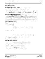
Page 24: ... PANEL PIXELS 8 bit Single Panel UD3 UD2 UD1 UD0 UD3 UD2 UD1 UD0 LD3 LD2 LD1 LD0 4 bit Single Panel UD3 UD2 UD1 UD0 LD3 LD2 LD1 LD0 Dual Panel Top Dual Panel Bottom 1 1 1 2 2 2 2 1 2 4 0 1 2 4 0 2 2 4 1 1 2 4 1 2 240 639 241 639 241 640 24 0 640 1 639 2 639 2 640 1 640 480 1 480 2 480 639 480 640 UP PER LCD PANEL TO P VIEW LO W ER LCD PANEL 640 DOTS 240 LINE S 240 LINES ...

Page 25: ... BIT SINGLE PANEL LP 240 PULSES LP XSCL UD 3 0 LINE 1 LINE 2 LINE 3 LINE 4 LINE 239 LINE 240 YD LINE 1 LINE 2 LP 4 PULSES LP WF UD2 1 2 1 6 1 318 UD1 1 3 1 7 1 319 UD0 1 4 1 8 1 320 UD3 1 1 1 5 1 317 WF X S C L 8 0 C L O C K P E R I O D S Example Timing for a 320x240 single panel ...

Page 26: ...L I N E 1 L I N E 2 L I N E 3 L I N E 4 L I N E 4 7 9 L I N E 4 8 0 YD L I N E 1 L I N E 2 LP WF UD2 1 2 1 10 1 634 UD1 1 3 1 11 1 635 UD0 1 4 1 12 1 636 LD3 1 5 1 13 1 637 LD2 1 6 1 14 1 638 LD1 1 7 1 15 1 639 LD0 1 8 1 16 1 640 UD3 1 1 1 9 1 633 WF LP 4 PULSES Example timing for a 640x480 panel X S C L 8 0 C L O C K P E R I O D S ...

Page 27: ...INE 2 242 LINE 3 243 LINE 4 244 LINE 239 479 LINE 240 480 YD LINE 1 241 LINE 2 242 LP WF UD2 1 2 1 6 1 638 UD1 1 3 1 7 1 639 UD0 1 4 1 8 1 640 LD3 241 1 241 5 241 637 LD2 241 638 LD1 241 639 LD0 241 640 UD3 1 1 1 5 1 637 X S C L 1 6 0 C L O C K P E R I O D S WF 241 2 241 6 241 3 241 7 241 4 241 8 LP 2 PULSES Example timing for a 640x480 panel ...

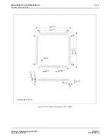
Page 28: ...ED1352 X16B C 001 06 22 PACKAGE DIMENSIONS Actual Size QFP5 100PIN S2 Unit mm SED1352 0 65 0 1 0 30 0 1 1 6 0 8 0 1 23 2 0 04 20 0 0 1 14 0 0 1 17 2 0 04 0 12 0 15 0 05 2 7 0 1 Index 100 1 30 31 50 51 80 81 0 35 ...

Page 29: ...GRAPHICS SED1352 X16B C 001 06 23 Actual Size QFP15 100PIN STD Unit mm SED1352F1B 1 25 75 51 50 26 76 100 Index 0 10 14 0 0 1 14 0 0 1 16 0 0 4 16 0 0 4 0 5 0 168 0 1 1 4 0 1 0 125 0 1 0 5 0 2 1 0 1 ...

Page 30: ...re 25 Harbour Road Wanchai Hong Kong Tel 2585 4600 Fax 2827 4346 Taiwan R O C Epson Taiwan Technology Trading Ltd 10F No 287 Nanking East Road Sec 3 Taipei Taiwan R O C Tel 02 2717 7360 Fax 02 2712 9164 Singapore Epson Singapore Pte Ltd No 1 Temasek Avenue 36 00 Millenia Tower Singapore 039192 Tel 337 7911 Fax 334 2716 Europe Epson Europe Electronics GmbH Riesstrasse 15 80992 Munich Germany Tel 08...

Page 31: ...ocument but only for your own use in evaluating Seiko Epson EPSON products You may not modify the document Epson Research and Development Inc disclaims any representation that the contents of this document are accurate or current The Programs Technologies described in this document may contain material protected under U S and or International Patent laws EPSON is a registered trademark of Seiko Ep...

Page 32: ...Page 2 Epson Research and Development Vancouver Design Center SED1352 Hardware Functional Specification X16 SP 001 16 Issue Date 99 07 28 THIS PAGE LEFT BLANK ...

Page 33: ...lock Descriptions 15 3 3 1 Bus Signal Translation 15 3 3 2 Control Registers 15 3 3 3 Sequence Controller 15 3 3 4 LCD Panel Interface 15 3 3 5 Look Up Table 16 3 3 6 Port Decoder 16 3 3 7 Memory Decoder 16 3 3 8 Data Bus Conversion 16 3 3 9 Address Generator 16 3 3 10 CPU CRT Selector 16 3 3 11 Display Data Formatter 16 3 3 12 Clock Inputs Timing 16 3 3 13 SRAM Interface 16 4 PINOUT DIAGRAM 17 5 ...

Page 34: ...ble Architecture 54 8 2 1 4 Level Gray Shade Mode 54 8 2 2 16 Level Gray Shade Mode 55 8 3 Power Save Modes PSM 1 55 8 3 1 Power Save Mode 1 PSM1 55 8 3 2 Power Save Mode 2 PSM2 56 8 3 3 Power Save Mode Function Summary 56 8 3 4 Pin States in Power Save Modes 56 9 DISPLAY MEMORY INTERFACE 57 9 1 SRAM Configurations Supported 57 9 1 1 8 Bit Mode 57 9 1 2 16 Bit Mode 59 9 2 SRAM Access Time 61 9 2 1...

Page 35: ...ble 7 7 MEMW Timing Non 68000 34 Table 7 8 MEMR Timing Non 68000 35 Table 7 9 Clock Input Requirements 36 Table 7 10 Write Data to Display Memory 37 Table 7 11 Read Data From Display Memory 38 Table 7 12 4 Bit Single LCD Interface Timing 40 Table 7 13 8 Bit LCD Interface Timing 41 Table 8 1 Maximum Value of Line Byte Count Register 8 Bit Display Memory Interface 48 Table 8 2 Maximum Value of Line ...

Page 36: ...Page 6 Epson Research and Development Vancouver Design Center SED1352 Hardware Functional Specification X16 SP 001 16 Issue Date 99 07 28 THIS PAGE LEFT BLANK ...

Page 37: ...35 Figure 18 Clock Input Requirements 36 Figure 19 Recommended Clock Interface 36 Figure 20 Write Data to Display Memory 37 Figure 21 Read Data From Display Memory 38 Figure 22 LCD Interface Timing 39 Figure 23 LCD Interface Pixel Data Position 42 Figure 24 4 Bit Single Monochrome Panel Timing 43 Figure 25 8 Bit Single Monochrome Panel Timing 44 Figure 26 8 Bit Dual Monochrome Panel Timing 45 Figu...

Page 38: ...Page 8 Epson Research and Development Vancouver Design Center SED1352 Hardware Functional Specification X16 SP 001 16 Issue Date 99 07 28 THIS PAGE LEFT BLANK ...

Page 39: ... designed for products where low cost low power consumption and low component count are the major design considerations This chip operates from 2 7 Volts to 5 5 Volts and up to 25MHz to suit different power consumption speed and cost requirements The SED1352 offers a flexible microprocessor interface The SED1352 is capable of displaying a maximum of 16 levels of gray A 16x4 Look Up Table is provid...

Page 40: ...accesses controlled by a READY or WAIT signal option to use built in index register or direct mapping to access one of fifteen internal registers 8 bit or 16 bit SRAM data bus interface configurations display memory configurations 128K bytes using one 64Kx16 SRAM 128K bytes using two 64Kx8 SRAMs 64K bytes using two 32Kx8 SRAMs 40K bytes using one 8Kx8 and one 32Kx8 SRAM 32K bytes using one 32Kx8 S...

Page 41: ... Display Support example resolutions 640x480 with 4 grays 640x400 with 16 grays passive monochrome LCD panels 4 bit single 4 bit data transfer 8 bit single 8 bit data transfer 8 bit dual 4 bit data transfer for each half panel 2 5 Power Management two software power save modes low power consumption panel power control switch see AUX 01h bit 4 ...

Page 42: ...the SED1352 All of the following block diagrams are shown without SRAM or LCD display Refer to interface specific Application Notes for complete details X16 AN xxx xx 3 1 16 Bit MC68000 MPU Figure 1 16 Bit 68000 Series example implementation only actual may vary SED1352 MEMCS IOCS MC68000 DTACK D0 to D15 A1 to A19 AB1 to AB19 DB0 to DB15 IOW IOR Decoder AS R W BHE UDS READY A20 to A23 AB0 LDS Deco...

Page 43: ...de example implementation only actual may vary MEMCS MEMW MEMR READY DB0 to DB7 AB0 to AB15 IOCS IOW IOR RESET SED1352 Z80 RESET D0 to D7 WAIT A0 to A15 WR RD Decoder IORQ A10 to A15 Decoder MREQ MI 8086 Maximum mode CLK READY RESET RDY MEMW MEMR READY DB0 to DB15 AB0 to AB15 IOW IOR RESET SED1352 8284A D0 to D15 T OE CLK S2 S1 S0 DEN MRDC AMWC IORC AIOWC DT R CLK READY RESET 8288 AB16 to AB19 M I...

Page 44: ...CS MEMW MEMR READY 8 Bit ISA Bus SMEMW SMEMR IOCHRDY REFRESH SA0 to SA19 SD0 to SD7 DB0 to DB7 AB0 to AB19 Decoder SA16 to SA13 IOCS IOW IOR RESET RESET SA10 to SA15 AEN IOW IOR Decoder 0WS optional Decoder SA 1 or 4 through SA9 SED1352 MEMCS MEMW MEMR READY 16 bit ISA Bus SMEMW SMEMR IOCHRDY REFRESH SA0 to SA19 SD0 to SD15 DB0 to DB15 AB0 to AB19 Decoder IOCS IOW IOR RESET RESET Decoder SA10 to S...

Page 45: ...by direct mapping or by using the built in internal index register 3 3 3 Sequence Controller The Sequence Controller generates horizontal and vertical display timings according to the configuration registers settings 3 3 4 LCD Panel Interface The LCD Interface performs frame rate modulation for passive monochrome LCD panels Bus Control Registers Signal Translation Port Memory Data Bus Timing Gener...

Page 46: ...maps the external data bus either 8 bit or 16 bit into the internal odd and even data bus 3 3 9 Address Generator The Address Generator generates display refresh addresses used to access display memory 3 3 10 CPU CRT Selector The CPU CRT Selector accesses the display memory from the CPU or the display refresh circuitry 3 3 11 Display Data Formatter The Display Data Formatter reads the display data...

Page 47: ...15 16 17 18 19 20 21 22 23 24 25 26 27 28 29 30 80 79 78 77 76 75 74 73 72 71 70 69 68 67 66 65 64 63 62 61 60 59 58 57 56 55 54 53 52 51 DB6 DB5 DB4 DB3 DB2 DB1 DB0 OSC2 OSC1 BHE READY MEMR MEMW MEMCS IOR IOW IOCS VOE LCDENB XSCL AB19 VA0 VA1 VA2 VA3 VA4 VA5 VA6 VA7 VA8 VA9 VA10 VD0 VD1 VD2 VD3 VD4 VD5 VD6 SED1352F0B DB7 V SS V DD DB8 DB9 DB10 DB11 DB12 DB13 DB15 AB0 AB1 AB2 AB3 AB4 AB5 AB6 AB7 A...

Page 48: ... 18 19 20 21 22 23 24 25 26 27 28 29 30 80 79 78 77 76 75 74 73 72 71 70 69 68 67 66 65 64 63 62 61 60 59 58 57 56 55 54 53 52 51 DB6 DB5 DB4 DB3 DB2 DB1 DB0 OSC2 OSC1 BHE READY MEMR MEMW MEMCS IOR IOW IOCS VOE LCDENB XSCL AB19 VA0 VA1 VA2 VA3 VA4 VA5 VA6 VA7 VA8 VA9 VA10 VD0 VD1 VD2 VD3 VD4 VD5 VD6 SED1352F1B DB7 VDD VSS DB8 DB9 DB10 DB11 DB12 DB13 DB15 AB0 AB1 AB2 AB3 AB4 AB5 AB6 AB7 AB8 AB9 AB1...

Page 49: ...B14 AB15 AB16 AB17 AB18 AB19 VA0 VA1 VA2 VA3 VA4 VA5 VA6 VA7 VA8 VA9 VA10 VD0 VD1 VD2 VD3 VD4 VD5 VD6 RESET WF LP YD LD0 LD1 LD2 LD3 UD0 UD1 UD2 UD3 VCS1 VCS0 VWE VA15 VA14 VA13 VA12 VA11 VD15 VD14 VD13 VD12 VD11 VD10 VD9 VD8 VDD VSS VD7 DB6 DB5 DB4 DB3 DB2 DB1 DB0 OSC2 OSC1 BHE READY MEMR MEMW MEMCS IOR IOW IOCS VOE LCDENB XSCL 1 10 20 30 40 50 60 70 80 90 100 Dummy Pad Dummy Pad Chip Size Chip T...

Page 50: ...00 2 071 49 VSS 2 071 1 670 14 AB5 0 140 2 071 50 VDD 2 071 1 850 15 AB6 0 281 2 071 51 VD8 1 850 2 071 16 AB7 0 423 2 071 52 VD9 1 670 2 071 17 AB8 0 566 2 071 53 VD10 1 496 2 071 18 AB9 0 712 2 071 54 VD11 1 330 2 071 19 AB10 0 860 2 071 55 VD12 1 168 2 071 20 AB11 1 012 2 071 56 VD13 1 012 2 071 21 AB12 1 168 2 071 57 VD14 0 860 2 071 22 AB13 1 330 2 071 58 VD15 0 712 2 071 23 AB14 1 496 2 071 ...

Page 51: ...XSCL 2 071 1 496 93 DB2 2 071 0 712 79 LCDENB 2 071 1 330 94 DB3 2 071 0 860 80 VOE 2 071 1 168 95 DB4 2 071 1 012 81 IOCS 2 071 1 012 96 DB5 2 071 1 168 82 IOW 2 071 0 860 97 DB6 2 071 1 330 83 IOR 2 071 0 712 98 DB7 2 071 1 496 84 MEMCS 2 071 0 566 99 VSS 2 071 1 670 85 MEMW 2 071 0 423 100 VDD 2 071 1 850 86 MEMR 2 071 0 281 101 Dummy Pad 2 071 2 071 87 READY 2 071 0 140 102 Dummy Pad 2 071 2 0...

Page 52: ... Data Strobe UDS pin of MC68000 In other bus interfaces this pin is connected to the system address bus AB1 AB19 I 13 31 10 28 TTL These pins are connected to the system address bus BHE I 91 88 TTLS In MC68000 MPU interface this pin is connected to the Lower Data Strobe LDS pin of MC68000 In other bus interfaces this pin is the Bus High Enable input for use with 16 bit system In 8 bit bus mode tie...

Page 53: ...lay memory data bus of even byte addresses and VD8 VD15 are connected to the display memory data bus of odd byte addresses The output drivers of these pins are placed in a high impedance state when RESET is high On the falling edge of RESET the values of VD0 VD15 are latched into the chip to configure various hardware options VD0 VD15 each have an internal pull down resistor see section Table 5 6 ...

Page 54: ... this signal is used to latch a row of display data in the LCD X drivers and to turn on the row driver Y driver WF MOD O 80 77 CO4 LCD backplane BIAS signal This output toggles according to the value programmed in AUX 05h YD FPFRAME O 78 75 CO4 Vertical scanning start pulse A logic 1 on this signal sampled by the LCD module on the falling edge of LP is used by the panel row driver Y driver to indi...

Page 55: ...terface No byte swap of high and low data bytes in 16 bit bus interface VD4 VD12 Select I O mapping address bits 1 9 These nine bits are latched on power up and are compared to the MPU address bits 1 9 A valid I O cycle combined with a valid address will enable the internal I O decoder Therefore both types of I O mapping are limited to even address boundaries to determine either the absolute or in...

Page 56: ...n Min Typ Max Units VDD Supply Voltage VSS 0V 2 7 3 0 3 3 5 0 5 5 V VIN Input Voltage VSS VDD V IOPR Operating Current fOSC 6 MHz 16 grays 3 0 3 5 7 0 mA TOPR Operating Temperature 40 25 85 C PTYP Typical Active Power Consumption fOSC 6 MHz 16 grays 9 0 11 55 35 0 mW Table 6 3 Input Specifications Symbol Parameter Condition Min Typ Max Units VIL Low Level Input Voltage VDD 4 5V VDD 3 0V VDD 2 7V 0...

Page 57: ...oltage Type 2 TS2 CO2 TS2D2 Type 3 TS3 Type 4 TS4 CO4 IOL 3mA IOL 6mA IOL 12mA VSS 0 3 V VOL 3 0V Low Level Output Voltage Type 2 TS2 CO2 TS2D2 Type 3 TS3 Type 4 TS4 CO4 IOL 3mA IOL 5 mA IOL 10mA VSS 0 3 V VOH 5 0V High Level Output Voltage Type 2 TS2 CO2 TS2D2 Type 3 TS3 Type 4 TS4 CO4 IOH 2 mA IOH 4 mA IOH 8 mA VDD 0 4 V VOH 3 3V Low Level Output Voltage Type 2 TS2 CO2 TS2D2 Type 3 TS3 Type 4 TS...

Page 58: ...rameters are based on a maximum 16MHz bus clock IOW Timing Figure 10 IOW Timing 68000 Table 7 1 IOW Timing 68000 3V 3 3V 5V Symbol Parameter Min Typ Max Min Typ Max Units t1 AB 9 1 valid before AS falling edge 10 0 ns t2 AB 9 1 hold from AS rising edge 20 10 ns t3 IOCS hold from AS rising edge 0 0 ns t4 UDS LDS valid before AS rising edge 30 20 ns t5 UDS LDS falling edge to DTACK falling edge 40 2...

Page 59: ...and IOCS valid before AS falling edge 10 0 ns t2a AB 9 1 hold from AS rising edge 20 10 ns t2b IOCS hold from AS rising edge 0 0 ns t3 AS falling edge to DTACK falling edge 35 25 ns t4 AS rising edge to DTACK hi z delay 45 25 ns t5 AS falling edge to DB 15 0 valid 80 60 ns t6 DB 15 0 hold from AS rising edge 25 20 ns t7 AS rising edge to DB 15 0 hi z delay 35 30 ns AB 9 1 AS R W VALID VALID t2a t3...

Page 60: ...7 3 MEMW Timing 68000 3V 3 3V 5V Symbol Parameter Min Typ Max Min Typ Max Units t1 AB 19 1 and MEMCS valid before AS falling edge 0 0 ns t2 AB 19 1 and MEMCS hold from AS rising edge 0 0 ns t3 AS falling edge to DTACK falling edge 3 5 MCLK 20 3 5 MCLK 10 ns t4 AS rising edge to DTACK hi z delay 45 22 ns t5 AS falling edge to DB 15 0 valid 120 140 ns t6 DB 15 0 hold from AS rising edge 0 0 ns AB 19...

Page 61: ...V 5V Symbol Parameter Min Typ Max Min Typ Max Units t1 AB 19 1 and MEMCS valid before AS falling edge 0 0 ns t2 AB 19 1 and MEMCS hold from AS rising edge 0 0 ns t3 AS falling edge to DTACK falling edge 3 5 MCLK 20 3 5 MCLK 10 ns t4 AS rising edge to DTACK hi z delay 42 20 ns t5 DTACK falling edge to DB 15 0 valid 20 20 ns t6 DB 15 0 hold from AS rising edge 54 28 ns t7 AS rising edge to DB 15 0 h...

Page 62: ...IOW Timing Non 68000 Table 7 5 IOW Timing Non 68000 3V 3 3V 5V Symbol Parameter Min Typ Max Min Typ Max Units t1 AB 9 0 BHE and IOCS valid before IOW falling edge 10 0 ns t2 AB 9 0 BHE and IOCS hold from IOW rising edge 20 10 ns t3 DB 15 0 setup to IOW rising edge 20 10 ns t4 DB 15 0 hold from IOW rising edge 20 10 ns t5 Pulse width of IOW 30 20 AB 9 0 IOCS IOW VALID VALID t2 t4 t3 t1 DB 15 0 BHE ...

Page 63: ...ming Non 68000 3V 3 3V 5V Symbol Parameter Min Typ Max Min Typ Max Units t1 AB 9 0 BHE and IOCS valid before IOR falling edge 10 0 ns t2 AB 9 0 BHE and IOCS hold from IOR rising edge 20 10 ns t3 IOR falling edge to DB 15 0 valid 80 60 ns t4 DB 15 0 hold from IOR rising edge 25 20 ns t5 IOR rising edge to DB 15 0 hi z delay 30 30 ns AB 9 0 IOCS IOR VALID VALID t2 t4 t5 t3 t1 DB 15 0 BHE Hi Z Hi Z ...

Page 64: ...e 7 7 MEMW Timing Non 68000 3V 3 3V 5V Symbol Parameter Min Typ Max Min Typ Max Unit s t1 AB 19 0 BHE and MEMCS valid before MEMW falling edge 0 0 ns t2 AB 19 0 BHE and MEMCS hold from MEMW rising edge 0 0 ns t3 MEMW falling edge to READY falling edge 30 20 ns t4 MEMW falling edge to DB 15 0 valid 120 140 ns t5 DB 15 0 hold from MEMW rising edge 0 0 ns t6 READY negated pulse width 3 5 MCLK 20 3 5 ...

Page 65: ... 3V 3 3V 5V Symbol Parameter Min Typ Max Min Typ Max Units t1 AB 19 0 BHE and MEMCS valid before MEMR falling edge 0 0 ns t2 AB 19 0 BHE and MEMCS hold from MEMR rising edge 0 0 ns t3 MEMR falling edge to READY falling edge 30 20 ns t4 READY rising edge to DB 15 0 valid 15 10 ns t5 DB 15 0 hold from MEMR rising edge 30 28 ns t6 MEMR rising edge to DB 15 0 hi z delay 30 30 ns t7 READY negated pulse...

Page 66: ...commended RC load values RL 2MΩ 5 CL 6 8 pF The figure below demonstrates both a crystal interface and an oscillator interface to the SED1352 Figure 19 Recommended Clock Interface Table 7 9 Clock Input Requirements Symbol Parameter Min Typ Max Units TOSC Input Clock Period CLKI 40 ns tPWH Input Clock Pulse Width High CLKI 40 60 TOSC tPWL Input Clock Pulse Width Low CLKI 40 60 TOSC tf Input Clock F...

Page 67: ... section 9 2 and 9 3 Table 7 10 Write Data to Display Memory 3V 3 3V 5V Symbol Parameter Min Typ Max Min Typ Max Units t1 Address cycle time MCLK 10 MCLK 10 ns t2 VA 15 0 VCS0 and VCS1 valid before VWE falling edge MCLK 2 20 MCLK 2 10 ns t3 VA 15 0 VCS0 and VCS1 hold from VWE rising edge 0 0 ns t4 Pulse width of VWE MCLK 2 5 MCLK 2 5 ns t5 VD 15 0 setup to VWE rising edge MCLK 2 20 MCLK 2 20 ns t6...

Page 68: ...From Display Memory Where MCLK period 1 fOSC or 2 fOSC or 4 fOSC depending on which mode the chip is in See sections 9 2 and 9 3 Table 7 11 Read Data From Display Memory 3V 3 3V 5V Symbol Parameter Min Typ Max Min Typ Max t1 Address cycle time MCLK 10 MCLK 10 t2 VA 15 0 VCS0 and VCS1 access time MCLK 50 MCLK 30 t3 VD 15 0 hold time 0 0 VA 15 0 VSC0 VSC1 INPUT INPUT INPUT t1 t2 t3 VD 15 0 VALID ...

Page 69: ...Issue Date 99 07 28 X16 SP 001 16 7 4 LCD Interface Timing Figure 22 LCD Interface Timing YD SED1352 outputs t1 t2 t4 t3 LP WF LP XSCL AUX 01h bit 5 0 XSCL AUX 01h bit 5 1 t7a t8 t9 t5 t6 t10 t12 t11 UD 3 0 LD 3 0 t13 t7b t8 t9 t10 t11 UD 3 0 LD 3 0 t12 1 2 1 2 SED1352 outputs t6b t6c 80 LP SED1352 outputs ...

Page 70: ...24 ns t3b LP pulse width R1 bit 5 1 5tOSC 24 ns t4 WF delay from LP falling edge 0 20 ns t5 LP setup to XSCL falling edge R1 bit 5 0 2tOSC 24 ns t6a LP hold from XSCL falling edge R1 bit 5 0 2tOSC 24 ns t6b XSCL falling edge to LP falling edge R1 bit 5 1 only 13tOSC 24 ns t7a LP negated to XSCL falling edge R1 bit 5 0 2tOSC 24 ns t7b LP negated to XSCL falling edge R1 bit 5 1 7tOSC 24 ns t8 XSCL p...

Page 71: ...5tOSC 24 ns t4 WF delay from LP falling edge 0 20 ns t5 LP setup to XSCL falling edge R1 bit 5 0 2tOSC 24 ns t6a LP hold from XSCL falling edge R1 bit 5 0 4tOSC 24 ns t6b XSCL falling edge to LP falling edge single panel mode R1 bit 5 1 only 15tOSC 24 ns t6c XSCL falling edge to LP falling edge dual panel mode R1 bit 5 1 only 31tOSC 24 ns t7a LP negated to XSCL falling edge R1 bit 5 0 4tOSC 24 ns ...

Page 72: ...ctional Specification X16 SP 001 16 Issue Date 99 07 28 LCD Interface Pixel Data Position Figure 23 LCD Interface Pixel Data Position 8 bit Single Panel UD3 UD2 UD1 UD0 UD3 UD2 UD1 UD0 LD3 LD2 LD1 LD0 4 bit Single Panel UD3 UD2 UD1 UD0 LD3 LD2 LD1 LD0 Dual Panel Top Dual Panel Bottom ...

Page 73: ...X16 SP 001 16 Figure 24 4 Bit Single Monochrome Panel Timing LP 240 P ULS ES LP XS CL UD 3 0 LINE 1 LINE 2 LINE 3 LINE 4 LINE 239 LINE 240 YD LINE 1 LINE 2 LP 4 PULSES LP WF UD2 1 2 1 6 1 318 UD1 1 3 1 7 1 319 UD0 1 4 1 8 1 320 UD3 1 1 1 5 1 317 WF X S C L 8 0 C L O C K P E R I O D S Example Timing for a 320x240 single panel ...

Page 74: ...ming LP 480 P ULS E S LP XS CL UD 3 0 LD 3 0 L I N E 1 L I N E 2 L I N E 3 L I N E 4 L I N E 4 7 9 L I N E 4 8 0 YD L I N E 1 L I N E 2 LP WF UD2 1 2 1 10 1 634 UD1 1 3 1 11 1 63 5 UD0 1 4 1 12 1 636 LD3 1 5 1 13 1 63 7 LD2 1 6 1 14 1 63 8 LD1 1 7 1 15 1 63 9 LD0 1 8 1 16 1 64 0 UD3 1 1 1 9 1 633 WF LP 4 PULSES Example timing for a 640x480 panel X S C L 8 0 C L O C K P E R I O D S ...

Page 75: ...ULS ES LP XS CL UD 3 0 LD 3 0 LINE 1 241 LINE 2 242 LINE 3 243 LINE 4 244 LINE 239 479 LINE 240 480 YD LINE 1 241 LINE 2 242 LP WF UD2 1 2 1 6 1 638 UD1 1 3 1 7 1 639 UD0 1 4 1 8 1 640 LD3 241 1 241 5 241 637 LD2 241 638 LD1 241 639 LD0 241 640 UD3 1 1 1 5 1 637 X S C L 1 6 0 C L O C K P E R I O D S WF 241 2 241 6 2 4 1 3 2 4 1 7 2 4 1 4 2 4 1 8 LP 2 PULSES Example timing for a 640x480 panel ...

Page 76: ... IOW I O mapped address 1 data write data to the indexed register or read data IOR I O mapped address 1 read the indexed register To perform a 16 bit I O access write data IOW I O mapped address index data write the index and data of the register to be accessed read data IOW I O mapped address index write to the indexed register IOR I O mapped address 1 read the indexed register Note Bits marked n...

Page 77: ...display When this bit 1 16 gray shades are displayed 4 bits pixel When this bit 0 4 gray shades are displayed 2 bits pixel This bit goes low on RESET bit 2 LCD Data Width Selects between 4 bit and 8 bit display data widths for single LCD mode When this bit 1 8 bit data transfer width is enabled When this bit 0 4 bit data transfer width is enabled In dual panel mode the data transfer width is force...

Page 78: ...T AUX 02h Line Byte Count Register LSB I O address 0010b Read Write Line Byte Count Bit 7 Line Byte Count Bit 6 Line Byte Count Bit 5 Line Byte Count Bit 4 Line Byte Count Bit 3 Line Byte Count Bit 2 Line Byte Count Bit 1 Line Byte Count Bit 0 Table 8 1 Maximum Value of Line Byte Count Register 8 Bit Display Memory Interface Display Mode Maximum Value of Line Byte Count Register Corresponding Maxi...

Page 79: ...ades with 8 bit memory interface This bit is ignored in the 16 bit mem ory interface bits 7 0 Total Display Line Count Bits 7 0 These are the 8 LSB of the 10 bit Total Display Line Count and represent the number of scan lines 1 to a maximum value of 3FFh or 1024 scan lines In single panel mode In dual panel mode Note Note that the value programmed partially determines the frame period and hence af...

Page 80: ...to the upper half of the display While in a single panel configuration screen 1 refers to the first screen of the Split Screen Display feature where two differ ent images screen 1 and screen 2 can be displayed at the same time on one display Note The absolute address into display memory is determined by the Memory Mapping Address which is set by VD13 VD15 see Table 5 6 Summary of Power On Re set O...

Page 81: ...ges screen 1 and screen 2 can be displayed at the same time on one display The Screen 2 Display Start Address is the memory address corresponding to the first pixel of the second image stored in display memory To display screen 2 refer to AUX 0Ah Screen 1 Display Line Count Register LSB below AUX 08h Screen 2 Display Start Address Register LSB I O address 1000b Read Write Screen 2 Display Start Ad...

Page 82: ...merical difference between the last address of a display line and the first address in the following line If the Address Pitch Adjustment is not equal to zero then a virtual screen is formed The size of the virtual screen is only limited by the available display memory The actual display output is a window that is part of the whole image stored in the display memory For example with 128K of displa...

Page 83: ...to Table 27 4 Level Gray Shade Mode Look Up Table Architecture on page 54 for formats bits 7 6 Bank Bits 1 0 In 4 level gray mode 2 bits pixel the 16 position palette is arranged into four 4 position banks These two bits control which bank is currently selected These bits have no effect in 16 level gray mode 4 bits pixel bits 5 4 ID Bits After power on or hardware reset these bits can be read to i...

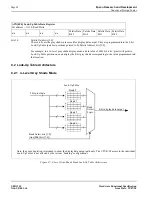
Page 84: ...shade corresponding to the value programmed into that location 8 2 Look Up Table Architecture 8 2 1 4 Level Gray Shade Mode Figure 27 4 Level Gray Shade Mode Look Up Table Architecture AUX 0Fh Look Up Table Data Register I O address 1111b Read Write n a n a n a n a Palette Data Bit 3 Palette Data Bit 2 Palette Data Bit 1 Palette Data Bit 0 Look Up Table 0 1 2 3 2 bit pixel data 0 1 2 3 0 1 2 3 0 1...

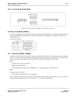
Page 85: ...s input clock frequency dependent the chip will enter State 2 The number of clocks of inactivity before entering State 2 is dependent on the display memory interface and the number of gray shades State 1 I O read write of all registers allowed Memory read write allowed LCD outputs are either forced low AUX 03h bit 5 0 or high impedance AUX 03h bit 5 1 State 2 The same as State 1 as well as Master ...

Page 86: ... Register AUX 03h bit 5 0 Table 8 6 Power Save Mode Function Summary Function Power Save Mode PSM Normal Active PSM1 PSM2 State 1 State 2 Display Active Yes No No No I O Access Possible Yes Yes Yes Yes Memory Access Possible Yes Yes No No Sequence Controller Running Yes No No No Internal Oscillator Disabled No No No Yes Table 8 7 Pin States in Power Save Modes Pin Pin State Normal Active PSM1 PSM2...

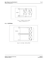
Page 87: ...e Date 99 07 28 X16 SP 001 16 9 DISPLAY MEMORY INTERFACE 9 1 SRAM Configurations Supported 9 1 1 8 Bit Mode Figure 29 8 Bit Mode 8K bytes SRAM Figure 30 8 Bit Mode 16K bytes SRAM Requires AUX 01h bit 0 0 8Kx8 SED1352 VWE VD0 7 VCS0 VCS1 VA0 12 WE CS n c 8Kx8 SED1352 VWE VD0 7 VCS0 VCS1 VA0 12 WE CS 8Kx8 WE CS ...

Page 88: ...6 Issue Date 99 07 28 Figure 31 8 Bit Mode 32K bytes SRAM Requires AUX 01h bit 0 1 Figure 32 8 Bit Mode 40K bytes SRAM either 8Kx8 32Kx8 requiring AUX 01h bit 0 0 or 32Kx8 8Kx8 requiring AUX 01h bit 0 1 32Kx8 SED1352 VWE VD0 7 VCS0 VCS1 VA0 14 WE CS n c 8K 32Kx8 SED1352 VWE VD0 7 VCS0 VCS1 VA0 14 WE CS 32K 8Kx8 WE CS ...

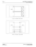
Page 89: ...fication SED1352 Issue Date 99 07 28 X16 SP 001 16 Figure 33 8 Bit Mode 64K bytes SRAM Requires AUX 01h bit 0 1 9 1 2 16 Bit Mode Figure 34 16 Bit Mode 16K bytes SRAM 32Kx8 SED1352 VWE VD0 7 VCS0 VCS1 VA0 14 WE CS 32Kx8 WE CS SED1352 VWE VD0 7 VD8 15 VCS0 VCS1 VA0 12 8Kx8 WE CS 8Kx8 CS WE ...

Page 90: ... Functional Specification X16 SP 001 16 Issue Date 99 07 28 Figure 35 16 Bit Mode 64K bytes SRAM Figure 36 16 Bit Mode 128K bytes SRAM SED1352 VWE VD0 7 VD8 15 VCS0 VCS1 VA0 14 32Kx8 WE CS 32Kx8 CS WE SED1352 VWE VD0 7 VD8 15 VCS0 VCS1 VA0 15 64Kx16 WE UB LB A0 15 I O 1 8 I O 9 16 ...

Page 91: ...y shades 2 bits per pixel system Memory Size bytes Table 9 1 8 Bit Display Memory Interface SRAM Access Time Display Mode 3V 3 3V 5V 16 level gray shades Access time 1 fOSC 50ns Access time 1 fOSC 30ns 4 level gray shades Access time 2 fOSC 50ns Access time 2 fOSC 30ns Table 9 2 16 Bit Display Memory Interface SRAM Access Time Display Mode 3V 3 3V 5V 16 level gray shades Access time 2 fOSC 50ns Ac...

Page 92: ...orted by SED1352 2 Memory more than 64KB can only be supported through 16 bit display memory interface KB K byte 1024 bytes Table 9 3 Memory Size Requirement Number of Horizontal Pixels 640 Number of Horizontal Pixels 640 4 Grays 2 bits per pixel 16 Grays 4 bits per pixel Example Display Memory Interface Size KB Access Time Size KB Access Time Input Clock fOSC Frame Rate 3V 3 3V 5V 3V 3 3V 5V Numb...

Page 93: ...ns 170 ns 370 ns 60 50 ns 150 ns 70 ns 170 ns 10 MHz 77 Hz 240 8 bit 16 bit 29 200 ns 450 ns 220 ns 470 ns 57 75 ns 200 ns 95 ns 220 ns 8 MHz 66 Hz 200 8 bit 16 bit 23 5 200 ns 450 ns 220 ns 470 ns 47 75 ns 200 ns 95 ns 220 ns 8 MHz 73 Hz Table 9 5 Memory Size Requirement Number of Horizontal Pixels 320 Number of Horizontal Pixels 320 4 Grays 2 bits per pixel 16 Grays 4 bits per pixel Example Disp...

Page 94: ...rdware Functional Specification X16 SP 001 16 Issue Date 99 07 28 10 MECHANICAL DATA Figure 37 Mechanical Drawing QFP5 100pin S2 All dimensions in mm 0 65 0 1 0 30 0 1 1 6 0 8 0 1 23 2 0 04 20 0 0 1 14 0 0 1 17 2 0 04 0 12 0 15 0 05 2 7 0 1 Index 100 1 30 31 50 51 80 81 0 35 ...

Page 95: ...nter Hardware Functional Specification SED1352 Issue Date 99 07 28 X16 SP 001 16 Figure 38 Mechanical Drawing QFP15 100pin All dimensions in mm 1 25 75 51 50 26 76 100 Index 0 10 14 0 0 1 14 0 0 1 16 0 0 4 16 0 0 4 0 5 0 168 0 1 1 4 0 1 0 125 0 1 0 5 0 2 1 0 1 ...

Page 96: ...Page 66 Epson Research and Development Vancouver Design Center SED1352 Hardware Functional Specification X16 SP 001 16 Issue Date 99 07 28 THIS PAGE LEFT BLANK ...

Page 97: ...ument but only for your own use in evaluating Seiko Epson EPSON products You may not modify the document Epson Research and Development Inc disclaims any representation that the contents of this document are accurate or current The Programs Technologies described in this document may contain material protected under U S and or International Patent laws EPSON is a registered trademark of Seiko Epso...

Page 98: ...Page 2 Epson Research and Development Vancouver Design Center SED1352 Programming Notes and Examples X16 BG 007 04 Issue Date 98 10 08 THIS PAGE LEFT BLANK ...

Page 99: ...MODELS 22 4 1 Registers 22 4 2 Description 24 4 2 1 SDU1352B0x Evaluation Board Display Memory 24 4 2 2 Display Start Address Registers 25 4 3 Common Display Memory Requirements for LCD Panel Sizes 27 5 ADVANCED TECHNIQUES 28 5 1 Virtual Displays 28 5 1 1 Registers 28 5 1 2 Description 29 5 2 Bitmaps and Text Displays 30 5 3 Registers 32 5 3 1 Indexed Addressing 32 5 3 2 Direct Addressing 32 5 4 S...

Page 100: ... Development Vancouver Design Center SED1352 Programming Notes and Examples X16 BG 007 04 Issue Date 98 10 08 6 PROGRAMMING THE SED1352 46 6 1 Main Loop Code 47 6 2 Initialization Code 48 6 3 Advanced Functions 52 7 GLOSSARY 65 ...

Page 101: ...s In One Byte of Display Memory 15 Figure 2 Pixel Storage for 4 Bits 16 gray shades in One Byte of Display Memory 15 Figure 3 4 Level Gray Shade Mode Look Up Table Architecture 20 Figure 4 16 Level Gray Shade Mode Look Up Table Architecture 21 Figure 5 Memory Map for 320 x 240 LCD Panel with 16 Gray Shades 25 Figure 6 Memory Map Example for 320 x 240 LCD Panel with 4 Gray Shades 27 Figure 7 Memory...

Page 102: ...Page 6 Epson Research and Development Vancouver Design Center SED1352 Programming Notes and Examples X16 BG 007 04 Issue Date 98 10 08 THIS PAGE LEFT BLANK ...

Page 103: ...ich describe the following Initializing the SED1352 Gray Shades and Look Up Tables Display Memory Models Virtual Displays Bitmaps and Text Displays Registers Split Screen Panning and Scrolling Power Saving The second half of this guide presents programming examples for the following Initialization Read Registers Gray Shades and Look Up Tables Text Split Screen Panning and Scrolling Power Saving Th...

Page 104: ... write one pixel to the top left corner of the display Program SED1352 Registers 00h 0Dh AUX Register Data in Binary Notes See Also AUX 00h 0000 0000 must be zero AUX 01h 1000 1000 b7 display on normal b6 single panel panel specific b5 XSCL not masked panel specific b4 LCDE LCDENB pin 0 implementation specific the recommended procedure is to turn this bit off during register initialization and aft...

Page 105: ...emory on page 24 and Section 4 1 Registers on page 22 AUX 0Ah 1110 1111 bits 7 0 bits 7 0 of Screen 1 Display Line Count application specific bits 9 8 of Screen 1 Display Line Count in bits 1 0 of AUX 0Bh application specific Screen 1 Display Line Count is typically the same as Total Display Line Count AUX 0Ah AUX 04h bits 1 0 of AUX 0Bh bits 1 0 of AUX 05h see Section 5 4 Split Screen on page 34 ...

Page 106: ...ochrome LUT data AUX 0Eh 0000 1100 increment palette address AUX 0Fh 0000 1100 write monochrome LUT data AUX 0Eh 0000 1101 increment palette address AUX 0Fh 0000 1101 write monochrome LUT data AUX 0Eh 0000 1110 increment palette address AUX 0Fh 0000 1110 write monochrome LUT data AUX 0Eh 0000 1111 increment palette address AUX 0Fh 0000 1111 write monochrome LUT data AUX 01h 1001 1000 Program Mode ...

Page 107: ...n specific AUX 02h 0100 1111 bits 7 0 bits 7 0 of Line Byte Count panel specific bit 8 of Line Byte Count in bit 0 of AUX 03h panel specific see Note A at end of Table for calculation AUX 03h 0000 0110 bits 7 6 Power Save Mode 0 application specific bit 5 LCD interface signals forced to 0 during Power Save implementation specific bit 4 no LUT bypass application specific bits 3 1 not used bit 0 bit...

Page 108: ...ay Memory on page 24 and Section 4 1 Registers on page 22 AUX 0Ah 1110 1111 bits 7 0 bits 7 0 of Screen 1 Display Line Count application specific bits 9 8 of Screen 1 Display Line Count in bits 1 0 of AUX 0Bh application specific Screen 1 Display Line Count is typically the same as Total Display Line Count AUX 0Ah AUX 04h bits 1 0 of AUX 0Bh bits 1 0 of AUX 05h see Section 5 4 Split Screen on page...

Page 109: ...1 increment palette address AUX 0Fh 0000 1100 write monochrome LUT data AUX 0Fh 0000 0000 write monochrome LUT data AUX 0Eh 0000 1101 increment palette address AUX 0Fh 0000 0101 write monochrome LUT data AUX 0Eh 0000 1110 increment palette address AUX 0Fh 0000 1010 write monochrome LUT data AUX 0Eh 0000 1111 select palette address AUX 0Fh 0000 1111 write monochrome LUT data AUX 01h 1001 1000 Progr...

Page 110: ... BG 007 04 Issue Date 98 10 08 Note A B Single Panel C Dual Panel Line Byte Count Panel Width in Pixels Memory Interface Width 8 or 16 bits bits per pixel 2 or 4 bits 1 640 16 2 1 79 4Fh Total Display Line Count number of display lines 1 Total Display Line Count number of display lines 2 1 480 2 1 239 0EFh ...

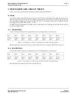
Page 111: ...ctions show how these pixels are stored in display memory 3 1 1 Two Bit Pixels To store two bit pixels four pixels are grouped into one byte of display memory as shown below Figure 1 Pixel Storage for 2 Bits 4 Gray Shades In One Byte of Display Memory When these pixels are shown Pixel 0 is seen to be left of Pixel 1 Pixel 1 is seen to be left of Pixel 2 and so on 3 1 2 Four Bit Pixels To store fou...

Page 112: ...hese two bits control which bank is currently selected These bits have no effect in 16 level gray mode 4 bits pixel bits 3 0 Palette Address Bits 3 0 These 4 bits provide a pointer into the 16 position Look Up Table currently selected for CPU R W access Note The Look Up Table configuration e g 1 2 4 banks does not affect the R W access from the CPU as all 16 positions can be accessed sequentially ...

Page 113: ... 4 bit wide LUTs The value inside each LUT entry represents the gray shade This value ranges between 0 and 15 The SED1352FOB Look Up Table is linear increasing the LUT entry number results in a lighter gray shade For example a LUT entry of 0Fh into a look up entry will always result in a bright white output An entry of 00h into a look up entry will always result in a black output Example 3 Initial...

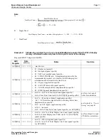
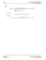
Page 114: ...to Look Up Table Address Register AUX 0Eh Read Old LUT Entry from Look Up Table Data Register AUX 0Fh 2 Calculate New LUT Entry according to the following formula 3 Write LUT entry back Write LUT index to Look Up Table Address Register AUX 0Eh Write New LUT Entry to Look Up Table Data Register AUX 0Fh 4 Repeat steps 1 to 3 until all 16 LUT entries have been changed If Table 3 1 was previously prog...

Page 115: ...6 entry LUT represent the first bank bank 0 The following four entries in the LUT rep resent the second bank bank 1 etc Consequently bank 2 starts at LUT index 8 as shown below Bank 2 is shown in Figure 3 palette 2 2 Write LUT index to Look Up Table Address Register AUX 0Eh For bank 2 the index will one of the following values 08h 09h 0Ah or 0Bh 3 Write LUT entry value to Look Up Table Data Regist...

Page 116: ...0 08 Figure 3 4 Level Gray Shade Mode Look Up Table Architecture 0 1 2 3 0 1 2 3 0 1 2 3 0 1 2 3 b3 b2 b1 b0 I1I0 Output Value to Gray Scale Engine 4 LUTs of 4 Entries x 4 Bits Bank Bits B1 B0 00 01 10 11 I1I0 I1I0 I1I0 I1I0 LUT Index 0 1 2 3 4 5 6 7 8 9 A B C D E F Display Data 2 Bits Pixel Palette 0 Palette 1 Palette 2 Palette 3 ...

Page 117: ...ay Shades Four Bits Pixel When the SED1352 has 4 bit pixels each pixel can index into one of 16 LUT entries The LUT bank bits are ignored in this mode Figure 4 16 Level Gray Shade Mode Look Up Table Architecture 0 1 2 3 4 5 6 7 8 9 A B C D E F b3 b2 b1 b0 I3I2I1I0 Output Value to Gray Scale Engine 1 LUT of 16 Entries x 4 Bits Display Data 4 Bits Pixel ...

Page 118: ...are the 16 most sig nificant bits of a 17 bit start address i e word access The Screen 1 Display Start Address is the memory address corresponding to the first displayed pixel top left corner In a dual panel configuration screen 1 refers to the upper half of the display While in a single panel configuration screen 1 refers to the first screen of the Split Screen Display feature where two differ en...

Page 119: ...es screen 1 and screen 2 can be displayed at the same time on one display The Screen 2 Display Start Address is the memory address corresponding to the first pixel of the second image stored in display memory To display screen 2 refer to AUX 0A Screen 1 Display Line Count Register LSB below AUX 08 Screen 2 Display Start Address Register LSB I O address 1000b Read Write Screen 2 Display Start Addr ...

Page 120: ... 128k of display memory display memory exists from address C000 0000h to address D000 FFFFh For the SDU1352B0x the Screen Display Start Address Registers are always in reference to the display memory address C000 0000h Writing 0 to a Display Start Address Register will always refer to C000 0000h even if display memory only exists from D000 0000h to D000 FFFFh Consequently if only 64k of display me...

Page 121: ... attached to the SDU1352B0x evaluation board with 64k of display memory 1 Calculate the number of bytes per scan line 2 Calculate the total number of bytes required for display memory 3 Create the memory map Each scan line is 00A0h bytes long there are 240 scan lines and the last memory address is 9600h 1 Figure 5 Memory Map for 320 x 240 LCD Panel with 16 Gray Shades 4 Program the Screen 1 Displa...

Page 122: ...he number of bytes per scan line 2 Calculate the total number of bytes required for display memory 3 Compare the required number of bytes with the amount of memory available to the SED1352 If the SED1352 has 128k available there is 131 072 bytes available which is greater than the 76 800 bytes re quired for 640 x 480 with 4 gray shades If the SED1352 has 64k available there is 65 536 bytes availab...

Page 123: ...y Map Example for 320 x 240 LCD Panel with 4 Gray Shades Figure 7 Memory Map Example for 640 x 200 LCD Panel with 16 Gray Shades Table 4 1 Memory Size Requirements Display Resolution Pixel Storage Memory Requirements Bits Pixel Gray Shades Bytes Hex 320x240 2 4 19 200 0000 4B00 4 16 38 400 0000 9600 640x200 2 4 32 000 0000 7D00 4 16 64 000 0000 FA00 640x480 2 4 76 800 0001 2C00 4 16 N A N A Offset...

Page 124: ...or example with 128K of display memory a 640x400 16 gray image can be stored If the output display size is 320x240 then the whole image can be seen by changing display starting addresses through AUX 06 and 07 and AUX 08 and 09 Note that a virtual screen can be produced on either a single or dual panel In 8 bit memory interface if the Address Pitch Adjustment is not equal to zero then a virtual scr...

Page 125: ... the Memory Interface is 16 bits 1 Initialize the SED1352 registers for a 320x240 panel 2 Determine whether the Address Pitch Adjustment Register refers to bytes or words Since the Memory Interface is set to 16 bits the Address Pitch Adjustment Register refers to words 3 Determine the number of pixels per unit referred to by the Address Pitch Adjustment Register The Address Pitch Adjustment Regist...

Page 126: ... Initialize the Look Up Table on page 17 3 Calculate the display memory map See Figure 5 Memory Map for 320 x 240 LCD Panel with 16 Gray Shades on page 25 4 Write font to display memory In a general purpose program the entire bitmapped font would be placed in an array As characters are to be dis played the program would choose the appropriate bitmap select the proper position on the screen and wri...

Page 127: ... 0 0 0 F F 0 0 0 F 0 F F 0 0 0 F F 0 F 0 F F 0 F 0 0 00AF 0140 0 0 F F 0 0 0 0 0 F F 0 F 0 0 0 0 F F 0 F F 0 0 0 0 F F 0 0 0 0 014F 01E0 0 0 F F 0 0 0 0 0 F F F F 0 0 0 0 0 F F F 0 0 0 0 0 F F 0 0 0 0 01EF 0280 0 0 F F 0 0 0 0 0 F F 0 F 0 0 0 0 0 F F F 0 0 0 0 0 F F 0 0 0 0 028F 0320 0 0 F F 0 0 0 0 0 F F 0 0 0 F 0 0 F F 0 F F 0 0 0 0 F F 0 0 0 0 032F 03C0 0 F F F F 0 0 0 F F F F F F F 0 F F 0 0 0...

Page 128: ...dresses are defined as Index Address and Data To access registers using this method an Index Address must be written to the first I O address location allowing data to be written read to from the second I O address Example 12 Write 12h to register 08h on the SDU1352B0x evaluation board the base port address is 310h and indexed port mapping is used 1 Write 08h to the index register The index regist...

Page 129: ... is 310h and direct port mapping is used 1 Calculate the port address for register 08h 2 Write the value 12h to port address 318h MOV DX 318h MOV AL 12h OUT DX AL Note The SDU1352B0x is normally configured for register indexing not direct mapping Refer to the SDU1352B0x Evaluation Board User s Manual for more information configuring the SDU1352B0x board for register indexing or register direct map...

Page 130: ...lines 1 For example if AUX 0A 20h for a 320x240 display system The display will show 20h 1 33 lines on the upper part of the screen according to display starting address AUX 06 and AUX 07 and 240 33 207 lines on the lower part of the screen according to display starting address AUX 08 and AUX 09 Two different images can be displayed when using a dual panel configuration by changing the screen 2 di...

Page 131: ... Registers refer to bytes or words Since the Memory Interface is set to 16 bits the Display Start Address Registers refer to words Note that when ad dresses refer to words the image must be aligned in memory such that the beginning is found on a word boundary the least significant bit of the memory address must be 0 2 Calculate the number of bytes per scan line 3 Determine the display memory locat...

Page 132: ... down the display If the line count is set to the maximum number of visible scan lines 1 only image 1 is shown AUX 0Ah LSB of visible scan lines 1 0EFh AUX 0Bh MSB of visible scan lines 1 00h If the line count is set to 0 then the first scan line of image 1 is shown followed by the first part of image 2 AUX 0Ah 00h AUX 0Bh 00h It is not possible to show only image 2 by changing the line count If o...

Page 133: ... first 100 scan lines of image 1 are shown following by the first part of im age 2 see Figure 12 AUX 0Ah 63h 99 decimal AUX 0Bh 00h Figure 12 320 x 240 Single Panel for Split Screen 9 Write both image 1 and image 2 to their respective locations in display memory Scan Line 0 Image 1 Scan Line 99 Scan Line 100 Image 2 Scan Line 239 Screen 1 Display Line Count Register 99 lines ...

Page 134: ...x this address is C000 0000h 4 Program the Screen 1 Display Start Address Register to point to the beginning of image 1 Since image 1 is at the beginning of display memory for a 128k system program the Screen 1 Display Start Address Register to 0000h AUX 06h 00h AUX 07h 00h 5 Calculate the total number of bytes required for image 1 6 Determine the display memory location for image 2 Place image 2 ...

Page 135: ...Address AUX 09h MSB of Screen 2 Display Start Address To pan image 1 to the right by a group of pixels the Screen 1 Start Address Register must be increased by 1 AUX 06h LSB of Screen 1 Display Start Address AUX 07h MSB of Screen 1 Display Start Address See Section 5 5 2 Panning Right and Left on page 42 for more information To pan image 2 to the left by a group of pixels the Screen 2 Start Addres...

Page 136: ...s must be 0 2 Calculate the number of bytes per scan line 3 Determine the display memory location for image 1 For simplicity assign the beginning of display memory as the starting address of image 1 see Figure 14 For the SDU1352B0x this address is C000 0000h Figure 14 Memory Map for a Dual Panel showing a Single Image 4 Program the Screen 1 Display Start Address Register to point to the beginning ...

Page 137: ...llows 7 Program the Screen 2 Display Start Address Register to point to the beginning of image 2 Image 2 is placed right after image 1 as shown below AUX 08h 00h AUX 09h 4Bh 8 Write both image 1 and image 2 to their respective locations in display memory image 2 address base display memory address size of image 1 C000 0000h 0000 9600h C000 9600h Screen 2 Display Start Address Register Screen 1 Dis...

Page 138: ...352 can pan right or left by either 2 4 or 8 pixels This is because the Screen 1 Display Start Address Register refers to either bytes or words see Section 4 2 1 SDU1352B0x Evaluation Board Display Memory on page 24 and a byte can represent either 2 or 4 pixels and so a word can represent 4 or 8 pixels see Table 5 1 below Table 5 1 Smallest Number of Pixels for Panning 5 5 3 Scrolling Up and Down ...

Page 139: ...o the Screen 2 Display Start Address Register In this example the Screen 2 Display Start Address has previously been initialized as described in Section 5 4 4 1 Displaying a Single Image on a Dual Panel on page 40 5 FOR DUAL PANELS ONLY Program the Screen 2 Display Start Address AUX 08h least significant byte of Screen 2 Display Start Address AUX 09h most significant byte of Screen 2 Display Start...

Page 140: ...ed for power reduction in hand held devices market These modes can be enabled by setting the 2 Power Save bits AUX 03h bits 7 6 The various settings are 5 6 2 1 Power Save Mode 1 Power Save Mode 1 would typically be used when power savings are required and memory accesses may occur The disad vantage is that since the oscillator is running this mode consumes more power that Power Save Mode 2 5 6 2 ...

Page 141: ...write operation so as not to destroy any other data in the register 2 Refer to the programming example in Advanced Functions on page 52 Table 5 4 Power Save Mode Function Summary Function Power Save Mode PSM Normal Active PSM1 PSM2 State 1 State 2 Display Active Yes No No No I O Access Possible Yes Yes Yes Yes Memory Access Possible Yes Yes No No Sequence Controller Running Yes No No No Internal O...

Page 142: ...ray shades in most of the examples This program accepts the following command line options DEMO type x n y n p n For example if there is a 320x240 single panel LCD with a port address of 310h type DEMO SINGLE x 320 y 240 p 310 When DEMO is started output will be sent to the standard output device This output will present a menu of numbered options Figure 15 Display for DEMO EXE where type SINGLE D...

Page 143: ...ESCRIPTION Start of demo program INPUTS Command line arguments RETURN VALUE None void main char argc char argv int ch CheckArguments argc argv printf Initializing n Initialize ClearLCDScreen ShowMenu while ch getch ESC switch ch case 1 ShowRegisters break case 2 GrayShadeBars break case 3 SplitScreen break case 4 PanScroll break case 5 PowerSaving break case ESC exit 0 ...

Page 144: ...PUTS The following global variables are changed PanelGrayLevel BytesPerScanLine void Initialize void static unsigned int val static unsigned int x PanelGrayLevel 16 Mode Register Display ON Panel SINGLE Mask XSCL NOT MASKED LCDE NOT ENABLED Gray Scale 16 Gray Shades 4 bits pixel LCD Data Width 8 bit data transfer Memory Interface 16 bits RAMS Addressing for 8Kx8 SRAM val 0x8C if PanelType TYPE_DUA...

Page 145: ... val 0xff Line Byte Word Count Register WriteRegister 3 val 8 0x01 Line Byte Word Count Power Save Reg BytesPerScanLine is a global variable BytesPerScanLine PanelX 2 For 16 gray shades only Total Display Line Count Register Screen 1 Display Line Count Register To show a full image on Screen 1 copy the Total Display Line Count into the Screen 1 Display Line Count Assume that all panels smaller tha...

Page 146: ...a dual panel the Screen 2 Display Start Address must point to the second half of the image in video memory if PanelType TYPE_DUAL val unsigned int ReadRegister 3 0x01 8 ReadRegister 2 val val PanelY 2 WriteRegister 8 val 0xff WriteRegister 9 val 8 else On a single panel Screen 1 was programmed to show all of its lines Consequently Screen 2 will not be seen and so the Screen 2 Display Start Address...

Page 147: ... to the address registers will effectively add 10000h bytes to the address Adding 10000h to C000 0000 will point to D000 0000 which is why this address correction works WriteRegister 7 0x80 MSB of Screen 1 Display Start Address val ReadRegister 9 MSB of Screen 2 Display Start Address val 0x80 WriteRegister 9 val Set Address Pitch Adjustment to 0 WriteRegister 0x0d 0 Write to Address Pitch Adjustme...

Page 148: ...registers INPUTS None RETURN VALUE None void ShowRegisters void static unsigned char x printf SED1352 Registers for x 0 x 16 x printf 02X ReadRegister x printf nSED1352 Look Up Table for x 0 x 16 x WriteRegister 0x0e x printf 02X ReadRegister 0x0f ShowMenu FUNCTION GrayShadeBars DESCRIPTION Displays one set of vertical bars each with a different gray shade INPUTS None RETURN VALUE None void GraySh...

Page 149: ...te Count register for 16 gray shades Since 16 gray shades corresponds to 2 pixels per byte there are x horizontal pixels 2 bytes per scan line This means that there are x horizontal pixels 4 words per scan line Since the Memory Interface is set to 16 bits the Line Byte Word Count refers to words val PanelX 4 1 BytesPerScanLine PanelX 2 WriteRegister 2 val 0xff Line Byte Count Register WriteRegiste...

Page 150: ...rt To display vertical bars this routine assumes that pVideo points to the beginning of a scan line In addition this routine assumes that the Address Pitch Adjustment Register is 0 no virtual display To write one vertical line first write one pixel to the first byte pointed to by pVideo Write the next pixel to the byte on the next scan line pointed to by pVideo BytesPerScanLine this only works if ...

Page 151: ...e character All other characters are replaced by spaces NOTES It is assumed that a pixel set to a value of 0 represents the background color black The character is translated to a block character void ShowText unsigned char _far pdisplayStart char str int color static const unsigned char pFont static unsigned char _far pdisplayFirstColumn static unsigned char _far pDisplay static unsigned char ch ...

Page 152: ...0xF0 0x00 P 0x78 0xCC 0xCC 0xCC 0xDC 0x78 0x1C 0x00 Q 0xFC 0x66 0x66 0x7C 0x6C 0x66 0xE6 0x00 R 0x78 0xCC 0xE0 0x70 0x1C 0xCC 0x78 0x00 S 0xFC 0xB4 0x30 0x30 0x30 0x30 0x78 0x00 T 0xCC 0xCC 0xCC 0xCC 0xCC 0xCC 0xFC 0x00 U 0xCC 0xCC 0xCC 0xCC 0xCC 0x78 0x30 0x00 V 0xC6 0xC6 0xC6 0xD6 0xFE 0xEE 0xC6 0x00 W 0xC6 0xC6 0x6C 0x38 0x38 0x6C 0xC6 0x00 X 0xCC 0xCC 0xCC 0x78 0x30 0x30 0x78 0x00 Y 0xFE 0xC6 ...

Page 153: ...if val 0x04 Display color 4 if val 0x02 Display color 2 if val 0x01 Display color pDisplay unsigned char Display pdisplayFirstColumn BytesPerScanLine pdisplayStart 2 Point to next character pdisplayFirstColumn pdisplayStart else 16 Gray Shades color 0x0f while str 0 ch str if ch Block character pFont font 1 0 else if ch A ch Z pFont font 0 0 else pFont font ch A 2 0 for y 0 y 8 y pDisplay pdisplay...

Page 154: ...ay 0 if val 0x10 Display color pDisplay unsigned char Display if val 0x08 Display color 4 else Display 0 if val 0x04 Display color pDisplay unsigned char Display if val 0x02 Display color 4 else Display 0 if val 0x01 Display color pDisplay unsigned char Display pdisplayFirstColumn BytesPerScanLine pdisplayStart 4 Point to next character pdisplayFirstColumn pdisplayStart FUNCTION SplitScreen DESCRI...

Page 155: ...on of image 1 ImageSize BytesPerScanLine PanelY Because the image size is limited to a maximum of 320 x 240 and there is 64k of video memory there is enough memory available FP_SEG pVideoImage2 0xd000 FP_OFF pVideoImage2 unsigned int ImageSize ShowVerticalBars pVideoImage1 ShowHorizontalBars pVideoImage2 Show text The lightest gray shade is set to PanelGrayLevel 1 ShowText pVideoImage1 SPLIT SCREE...

Page 156: ...MaxVirtualScanLines unsigned int unsigned long 0x10000 BytesPerScanLine MinLineCount OriginalLineCount MaxVirtualScanLines OriginalLineCount 1 Delay 0 5 Scroll image 2 down for val MinLineCount val OriginalLineCount val 1 WriteRegister 0x0a val 0xff Total Display Line Count WriteRegister 0x0b val 8 0x03 Total Disp Line Cnt WF Count Delay 0 1 Scroll image 2 up for val OriginalLineCount val MinLineC...

Page 157: ...tic unsigned int val pitch static unsigned char _far pVideo printf Showing Panning and Scrolling n Initialize ClearLCDScreen This pitch is calculated for 16 gray shades pitch VIRTUAL_X 2 BytesPerScanLine 2 WriteRegister 0x0d pitch BytesPerScanLine VIRTUAL_X 2 For 64k only FP_SEG pVideo 0xd000 FP_OFF pVideo 0x0000 Display random blocks of data To do so a text character will be used This character s...

Page 158: ...Text pVideo rand 16 ShowBorders Move virtual display from 0 0 to MaxX 0 MaxX VIRTUAL_X PanelX MaxY VIRTUAL_Y PanelY for x 0 x MaxX x SetStartAddress x 0 Delay 0 1 for y 0 y MaxY y SetStartAddress MaxX y Delay 0 1 for x MaxX x 0 x SetStartAddress x MaxY Delay 0 1 for y MaxY y 0 y SetStartAddress 0 y Delay 0 1 SetStartAddress 0 0 FUNCTION PowerSaving DESCRIPTION Starts power saving mode 2 INPUTS Non...

Page 159: ...ing n getch val 0x38 WriteRegister 3 val Cancel power saving mode 2 FUNCTION PowerSaving DESCRIPTION Starts power saving mode 2 INPUTS None RETURN VALUE None This is an optional method of power saving void PowerSaving void static unsigned int val printf Starting Power Saving n The following are the steps to enter a power save mode Step 1 Turn off display val ReadRegister 1 val 0x7f WriteRegister 1...

Page 160: ...ister 3 val 0x3f val 0x80 WriteRegister 3 val Set power saving mode 2 printf Press any key to cancel power saving n getch The following are the steps to exit a power save mode Step 1 Exit Power Save Mode val ReadRegister 3 val 0x3f WriteRegister 3 val Cancel power saving mode 2 Step 2 Enable LCDE turn on LCD power supply For the SDU1353B0C set LCDE bit to 1 val ReadRegister 1 val 0x10 WriteRegiste...

Page 161: ...ea of an LCD display which supports a single image LCD displays may have one or two panels panning The right or left movement of the viewport in a virtual display pixel Picture Element A pixel is seen as a dot on the display and can be shown using one of several different gray shades Combining pixels in a group creates an image power saving A means of reducing the power consumption of the SED1352 ...

Page 162: ...Page 66 Epson Research and Development Vancouver Design Center SED1352 Programming Notes and Examples X16 BG 007 04 Issue Date 98 10 08 THIS PAGE LEFT BLANK ...

Page 163: ...ment but only for your own use in evaluating Seiko Epson EPSON products You may not modify the document Epson Research and Development Inc disclaims any representation that the contents of this document are accurate or current The Programs Technologies described in this document may contain material protected under U S and or International Patent laws EPSON is a registered trademark of Seiko Epson...

Page 164: ...Page 2 Epson Research and Development Vancouver Design Center SED1352 1352SHOW EXE Display Utility X16 UI 001 08 Issue Date 98 10 08 THIS PAGE LEFT BLANK ...

Page 165: ...played i will invert all displayed images show as negative produces the usage message Examples 1352show with no arguments will run the program in split screen mode This will display two predefined images with screen one displaying horizontal bars and screen two displaying vertical bars Screen two may be scrolled up and down using the arrow page up page down home and end keys 1352show picture1 gif ...

Page 166: ...format must be 16 color non interlaced GIF89a format 1352SHOW will clear the screen when the Esc key is pressed Program Messages ERROR Split screen available for single panel only Split screen viewing is only allowed on single panels ERROR This program requires BIOS1352 to be loaded The program BIOS1352 COM must be run before 1352SHOW Load BIOS1352 COM and re run 1352SHOW EXE File filename not fou...

Page 167: ...ment but only for your own use in evaluating Seiko Epson EPSON products You may not modify the document Epson Research and Development Inc disclaims any representation that the contents of this document are accurate or current The Programs Technologies described in this document may contain material protected under U S and or International Patent laws EPSON is a registered trademark of Seiko Epson...

Page 168: ...Page 2 Epson Research and Development Vancouver Design Center SED1352 VIRTUAL EXE Display Utility X16 UI 002 08 Issue Date 08 10 08 THIS PAGE LEFT BLANK ...

Page 169: ...x n y n Where x is the horizontal resolution in multiples of 8 y is the vertical resolution produces a usage message If the user does not provide the virtual size the program will automatically select the size based on memory and panel size The user can then navigate throughout the image using the arrow keys to pan and scroll the screen Pressing the ESC key terminates the program Comments VIRTUAL ...

Page 170: ...play The virtual display is too large to fit in memory Choose a smaller x or y value ERROR Horizontal resolution must be a multiple of 8 Panning moves in multiples of pixels Choose a horizontal resolution which is a multiple of 8 so panning will not suffer from screen wrap around ERROR Specified horizontal resolution is smaller than panel resolution The virtual display must always be larger than t...

Page 171: ... but only for your own use in evaluating Seiko Epson EPSON products You may not modify the document Epson Research and Development Inc disclaims any representation that the contents of this document are accurate or current The Programs Technologies described in this document may contain material protected under U S and or International Patent laws EPSON is a registered trademark of Seiko Epson Cor...

Page 172: ...Page 2 Epson Research and Development Vancouver Design Center SED1352 BIOS1352 COM Utility X16 UI 003 08 Issue Date 98 10 08 THIS PAGE LEFT BLANK ...

Page 173: ...Program Requirements Installation Copy the file bios1352 com to a directory that is in the DOS path on your hard drive Usage BIOS1352 COM is run from the DOS command line as follows bios1352 type x n y n g n p n m n Where type is the panel type single for single panel or dual for dual panel x is the horizontal panel size in pixels decimal y is the vertical panel size in lines decimal g is the numb...

Page 174: ...ified for the panel in the command line ERROR Panels greater than 480 lines not supported More than 480 vertical lines has been specified for the panel in the command line ERROR Invalid port specified The port address p must be specified in the format 3x0 in the command line The range is 300h to 370h in 10h increments ERROR Only 4 or 16 gray shades allowed A number other than 4 or 16 has been spec...

Page 175: ...ment but only for your own use in evaluating Seiko Epson EPSON products You may not modify the document Epson Research and Development Inc disclaims any representation that the contents of this document are accurate or current The Programs Technologies described in this document may contain material protected under U S and or International Patent laws EPSON is a registered trademark of Seiko Epson...

Page 176: ...Page 2 Epson Research and Development Vancouver Design Center SED1352 1352GRAY EXE Display Utility X16 UI 004 08 Issue Date 98 10 08 THIS PAGE LEFT BLANK ...

Page 177: ...elect 1 of 4 palettes Program Requirements Installation Copy the file 1352gray exe to a directory that is in the DOS path on your hard drive Usage 1352GRAY is invoked from the DOS command line as follows 1352gray Where produces a usage message 1352GRAY displays a default gray shade pattern as a series of vertical or horizontal bars The pattern number of gray shades and current palette may be modif...

Page 178: ...352GRAY requires BIOS1352 COM to be loaded prior to running Four gray shades is always possible Switching to 16 gray shades may not be possible if the panel size exceeds 640x400 Program Messages ERROR This program requires BIOS1352 to be loaded The program BIOS1352 COM must be run before 1352GRAY Load BIOS1352 COM and then re run 1352GRAY EXE ...

Page 179: ...ument but only for your own use in evaluating Seiko Epson EPSON products You may not modify the document Epson Research and Development Inc disclaims any representation that the contents of this document are accurate or current The Programs Technologies described in this document may contain material protected under U S and or International Patent laws EPSON is a registered trademark of Seiko Epso...

Page 180: ...Page 2 Epson Research and Development Vancouver Design Center SED1352 1352PD EXE Power Down Utility X16 UI 005 07 Issue Date 98 10 08 THIS PAGE LEFT BLANK ...

Page 181: ... is run from the DOS command line as follows 1352pd ModeNumber Where ModeNumber is a decimal number 0 1 or 2 for the desired power down mode Example typing the following command line activates power down mode 2 1352pd 2 ENTER Output from the program can be redirected to an external DOS device such as a terminal attached to the serial port such as COM1 as shown below 1352pd 2 com1 ENTER Striking an...

Page 182: ...engage power down mode 1 or 2 SED1352 LUT will be disabled and all LCD signals are forced low Program Messages Power Down Mode xx is set The power down mode xx has been set This message may not be visible if the active display controller is the SED1352 ERROR Cannot set power mode xx 1352PD EXE cannot set the power down mode requested The power down mode must be 0 1 or 2 ERROR This program requires...

Page 183: ...cument but only for your own use in evaluating Seiko Epson EPSON products You may not modify the document Epson Research and Development Inc disclaims any representation that the contents of this document are accurate or current The Programs Technologies described in this document may contain material protected under U S and or International Patent laws EPSON is a registered trademark of Seiko Eps...

Page 184: ...Page 2 Epson Research and Development Vancouver Design Center SED1352 1352READ EXE Diagnostic Utility X16 UI 006 06 Issue Date 98 10 08 THIS PAGE LEFT BLANK ...

Page 185: ...filter such as MORE COM Installation Copy the file 1352read exe to a directory that is in the DOS path on your hard drive Usage From DOS prompt type the following 1352read port Where 1352read without any argument will read the SED1352 registers including the gray shade lookup table port is the SED1352 port address in hex e g 310 produces a usage message Example to generate a report simply type 135...

Page 186: ...tting for BIOS1352 and or 1352READ to ensure it is correct and re run the program ERROR 1352READ requires a port address 1352READ has not detected BIOS1352 COM to obtain the port address and no port address was specified on the command line Either specify a port address on the 1352READ command line or run BIOS1352 COM prior to running 1352READ ERROR BIOS1352 reports a port address of port which is...

Page 187: ... this document but only for your own use in evaluating Seiko Epson EPSON products You may not modify the document Epson Research and Development Inc disclaims any representation that the contents of this document are accurate or current The Programs Technologies described in this document may contain material protected under U S and or International Patent laws EPSON is a registered trademark of S...

Page 188: ...Page 2 Epson Research and Development Vancouver Design Center SED1352 SDU1352B0C Rev 1 0 Evaluation Board User Manual X16 AN 002 09 Issue Date 98 10 07 THIS PAGE LEFT BLANK ...

Page 189: ...nfiguration 8 1 3 Technical Description 12 1 3 1 ISA Bus Support 12 1 3 2 Non ISA Bus Support 13 1 3 3 SRAM Support 13 1 3 4 Monochrome LCD Support 13 1 3 5 Power Save Modes 13 1 3 6 Adjustable LCD Panel Negative Power Supply 13 1 3 7 Adjustable LCD Panel Positive Power Supply 14 1 3 8 Crystal Support 14 1 3 9 CPU Bus Interface Header Strips 14 1 3 10 Schematic Notes 14 Appendix A PARTS LIST 15 Ap...

Page 190: ...Page 4 Epson Research and Development Vancouver Design Center SED1352 SDU1352B0C Rev 1 0 Evaluation Board User Manual X16 AN 002 09 Issue Date 98 10 07 THIS PAGE LEFT BLANK ...

Page 191: ...ector J1 Pinout 9 Table 1 5 CPU BUS Connector H1 Pinout 10 Table 1 6 CPU BUS Connector H2 Pinout 11 List of Figures Figure 1 SDU1352B0C Rev 1 0 Schematic Diagram 1 of 7 16 Figure 2 SDU1352B0C Rev 1 0 Schematic Diagram 2 of 7 17 Figure 3 SDU1352B0C Rev 1 0 Schematic Diagram 3 of 7 18 Figure 4 SDU1352B0C Rev 1 0 Schematic Diagram 4 of 7 19 Figure 5 SDU1352B0C Rev 1 0 Schematic Diagram 5 of 7 20 Figu...

Page 192: ...Page 6 Epson Research and Development Vancouver Design Center SED1352 SDU1352B0C Rev 1 0 Evaluation Board User Manual X16 AN 002 09 Issue Date 98 10 07 THIS PAGE LEFT BLANK ...

Page 193: ... All appropriate components are surface mount to reduce cost and minimize board space 1 1 Features 100 pin QFP5 package SMD technology for all appropriate devices Monochrome STN LCD support 8 bit and 16 bit ISA Bus support 5V operation Two terminal crystal support up to 25 175MHz 16 bit wide 128K bytes SRAM support Configuration Options Support for Software Power Save Modes On board adjustable LCD...

Page 194: ...When using direct mapping I O the I O address is 0000 0011 0 xxxx where x is don t care and can be configured with dip switch SW1 5 through SW1 7 If 001 then the I O address for AUX 00h 0310h I O address for AUX 01h 0311h I O address for AUX 02h 0312h and so on Note These jumpers are necessary for the external ISA Bus decode logic Table 1 1 Configuration DIP Switch Settings Switch Signal Closed Op...

Page 195: ...LD3 7 LD3 UD0 9 UD0 UD0 Upper panel display data for dual panel dual drive mode In 8 bit single panel single drive mode these are the most significant 4 bits of the 8 bit output data to the panel data 7 4 In 4 bit single panel mode these are the 4 data bits output to the panel UD1 11 UD1 UD1 UD2 13 UD2 UD2 UD3 15 UD3 UD3 N C 17 31 odd pins XSCL 33 XSCL XSCL Shift Clock for LCD data NC 35 LP 37 LP ...

Page 196: ...D7 Connected to DB7 of the SED1352 11 GND Ground 12 GND Ground 13 SD8 Connected to DB8 of the SED1352 14 SD9 Connected to DB9 of the SED1352 15 SD10 Connected to DB10 of the SED1352 16 SD11 Connected to DB11 of the SED1352 17 GND Ground 18 GND Ground 19 SD12 Connected to DB12 of the SED1352 20 SD13 Connected to DB13 of the SED1352 21 SD14 Connected to DB14 of the SED1352 22 SD15 Connected to DB15 ...

Page 197: ...ected to AB8 of the SED1352 12 SA9 Connected to AB9 of the SED1352 13 SA10 Connected to AB10 of the SED1352 14 SA11 Connected to AB11 of the SED1352 15 SA12 Connected to AB12 of the SED1352 16 SA13 Connected to AB13 of the SED1352 17 GND Ground 18 GND Ground 19 SA14 Connected to AB14 of the SED1352 20 SA15 Connected to AB14 of the SED1352 21 SA16 Connected to AB16 of the SED1352 22 SA17 Connected ...

Page 198: ...set as desired SW1 8 closed 64K bytes available at D000h segment JP1 2 3 shorted to reflect SW1 8 polarity If using the SDU1352B0C in conjunction with a monochrome display adapter all 128K bytes of memory is available residing at segment C000h D000h The SDU1352B0C can be used as a stand alone video adapter with 128K bytes memory available If used as a stand alone video adapter the BIOS setup progr...

Page 199: ... Single monochrome STN LCD panels All the necessary signals are provided on the 40 pin ribbon cable header The interface signals are alternated with grounds on the cable to reduce cross talk and noise related problems Refer to Table 1 4 LCD Signal Connector J1 Pinout on page 9 for specific settings 1 3 5 Power Save Modes The SED1352 supports 2 software Power Save Modes The utility program 1352PD E...

Page 200: ...2 Determine the panel s specific power requirements and set the potentiometer accordingly before connecting the panel 1 3 8 Crystal Support The input crystal frequency may be up to 25 175MHz depending on the specific panel size and frame rate desired Refer to Section 9 3 of the SED1352 Functional Specification Drawing Office No X16 SP 001 xx for further details 1 3 9 CPU Bus Interface Header Strip...

Page 201: ...ohm 1206 pckg 1 13 4 R2 R15 R18 R21 1K 1206 pckg 5 14 2 R9 R10 10K 9 resistors resistor network Bourne 4610 101 103 or equivalent 15 4 R11 R14 10K 1206 pckg 5 16 1 R16 100 ohm 1206 pckg 5 17 1 R17 500 ohm Trim Pot Bourns 3386W 1 501 or equivalent 18 1 R19 100K Trim Pot Bourns 3386W 1 104 or equivalent 19 2 R20 R22 100K 1206 pckg 5 20 1 R24 240 ohm 1206 pckg 5 21 2 S1 S2 SW DIP 8 Dip Switch 8 posit...

Page 202: ...DB13 9 DB14 10 DB15 11 LD0 77 LD1 76 LD2 75 LD3 74 UD0 73 UD1 72 UD2 71 UD3 70 YD 78 LP 79 WF 80 XSCL 81 VA1 34 VA2 35 VA3 36 VA4 37 VA5 38 VA6 39 VA7 40 VA8 41 VA9 42 VA12 63 VA13 64 VA14 65 VA15 66 VD0 44 VD1 45 VD2 46 VD3 47 VD4 48 VD5 49 VD6 50 VD7 51 VD8 54 VD9 55 VD10 56 VD11 57 VD12 58 VD13 59 VD14 60 VD15 61 VWE 67 VOE 83 VCS0 68 VCS1 69 VA11 62 LCDENB 82 VA0 33 VA10 43 AB16 28 AB18 30 BHE...

Page 203: ...0 SA11 SA12 SA13 SA14 SA15 SA16 SA17 SA18 SA19 SA 1 19 128K 0FORUSINGALL128K 1 2 3 JP4 HEADER3 1 2 3 JP3 HEADER3 5V 128K FROMSW1 8 128K 128K 1FORUSINGUPPER64K P0 2 P1 4 P2 6 P3 8 P4 11 P5 13 P6 15 P7 17 Q0 3 Q1 5 Q2 7 Q3 9 Q4 12 Q5 14 Q6 16 Q7 18 G 1 P Q 19 U3 74LS688 5V SA6 SA7 SA8 SA9 ADDBIT4 ADDBIT5 ADDBIT6 1 2 3 U5A 74LS09 R2 100K 5V R1 1K MEMCS16 LCDPWR IOCS16 4 5 6 U5B 74LS09 9 10 8 U5C 74LS...

Page 204: ...VD7 IOBIT4 NOBYTESWAP ISA INDEXING 8BITBI A0 20 A1 19 A2 18 A3 17 A4 16 A5 15 A6 14 A7 13 A8 3 A9 2 A10 31 A11 1 A12 12 A13 4 A14 11 OE 32 DO1 21 DO2 22 DO3 23 DO4 25 DO5 26 DO6 27 DO7 28 DO8 29 A15 7 WE 5 CS1 30 CS2 6 VDD 8 VSS 24 A16 10 NC 9 U7 SRM20100LTM 70 5V 5V VD8 VD9 VD10 VD11 VD12 VD13 VD14 VD15 VA0 VA1 VA2 VA3 VA4 VA5 VA6 VA7 VA8 VA9 VA10 VA11 VA12 VA13 VA14 VA15 VA0 VA1 VA2 VA3 VA4 VA5 ...

Page 205: ...0A LD0 LD1 LD2 LD3 UD0 UD1 UD2 UD3 LD0 LD1 LD2 LD3 UD0 UD1 UD2 UD3 MonoLCDConnector XSCL LP YD XSCL YD LP 12V LCDPWR VDDH WF LCDPWR WF SA1 SA3 SA5 SA7 SA9 SA11 SA13 SA15 SA17 SA19 IOR SMEMR 5V GND GND GND SA0 SA2 SA4 SA6 SA8 SA10 SA12 SA14 SA16 SA18 IOW SMEMW 5V GND GND GND 3 5 7 9 11 13 15 17 19 21 23 25 27 29 31 2 4 6 8 10 12 14 16 18 20 22 24 26 28 30 32 1 H2 CON32A SD1 SD3 SD5 SD7 SD9 SD11 SD1...

Page 206: ...D2 7 SD1 8 SD0 9 IOCHRDY 10 AEN 11 SA19 12 SA18 13 SA17 14 SA16 15 SA15 16 SA14 17 SA13 18 SA12 19 SA11 20 SA10 21 SA9 22 SA8 23 SA7 24 SA6 25 SA5 26 SA4 27 SA3 28 SA2 29 SA1 30 SA0 31 AT1 ATCON A SD7 SD6 SD5 SD4 SD3 IOCHRDY IOEN SD2 SD1 SD0 SA19 SA18 SA17 SA16 SA15 SA14 SA13 SA12 SA11 SA10 SA9 SA8 SA7 SA6 SA5 SA4 SA3 SA2 SA1 SA0 12V SMEMW SMEMR IOW IOR REFRESH MEMCS16 IOCS16 5V MEMCS16 1 IOCS16 2...

Page 207: ...ble23vto40v L1 1uH 5V V O U T _ A D J 1 D C _ I N 2 R E M O T E 3 G N D 4 G N D 5 G N D 6 G N D 7 G N D 8 N C9 G N D 1 0 G N D 1 1 D C _ O U T 1 2 U8 RD 0412 R7 470K C1 56uF 35V 1 3 2 R8 200k R10 14k 5V C2 10uF 63V C3 10uF 63V C4 10uF 63V LOWESR LOWESR 2 1 3 Q1 2N3905 2 1 3 Q2 2N3903 VLCD adjustable 18vto 23v R13 1K R12 100K R14 1K R15 100K 5V D C _ O U T 1 D C _ O U T 2 N C3 G N D 4 G N D 5 V O U...

Page 208: ...et 7 of 7 Size DocumentNumber REV B X16 SCH 002 1 0 Title SDU1352B0C S MOSSYSTEMS INC VDC 5V Whentheoscillatorpackageis used thestabilizingcapacitors andresistormustberemoved NC 1 OUT 8 GND 7 VCC 14 U10 OSC 14 OSC1 OSC2 1 4 Y1 25 175Mhz R16 2M 5V BYPASSCAPACITORS 1 POWERPIN C7 7pF C8 7pF C18 1uF C19 1uF C20 1uF C21 1uF C22 1uF 12V C14 1uF C15 1uF C16 1uF C17 1uF 5V C13 1uF C11 1uF C12 1uF 12V 12V ...

Page 209: ...but only for your own use in evaluating Seiko Epson EPSON products You may not modify the document Epson Research and Development Inc disclaims any representation that the contents of this document are accurate or current The Programs Technologies described in this document may contain material protected under U S and or International Patent laws EPSON is a registered trademark of Seiko Epson Corp...

Page 210: ...Page 2 Epson Research and Development Vancouver Design Center SED1352 Power Consumption X16 AN 006 06 Issue Date 98 10 08 THIS PAGE LEFT BLANK ...

Page 211: ...z screen pattern 00h and AAh on 480x320 single panel 3 Pixel clock 6MHz screen pattern 00h and AAh on 320x240 single panel 4 No display connected Active Pattern 00h Active Pattern AAh PD1 PD2 Units 25MHz 93 0 105 5 14 3 0 1 mW 12MHz 58 7 66 1 11 8 0 1 mW 6MHz 32 7 36 1 4 7 0 0 mW 100 80 60 40 20 0 ACTIVE Pattern 00h ACTIVE Pattern AAh PD1 PD2 Operating Mode Power mW SED1352 Power Consumption VDD 5...

Page 212: ...10 08 Active Pattern 00h Active Pattern AAh PD1 PD2 Units 25MHz 35 0 41 2 3 3 0 2 mW 12MHz 16 1 18 1 2 2 0 3 mW 6MHz 8 3 9 5 0 2 0 0 mW 40 35 30 25 20 15 10 5 0 SED1352 Power Consumption VDD 3 0V ACTIVE Pattern 00h ACTIVE Pattern AAh PD1 PD2 Operating Mode Power mW 25MHz Pixel Clock 12MHz Pixel Clock 6MHz Pixel Clock ...

Page 213: ...document but only for your own use in evaluating Seiko Epson EPSON products You may not modify the document Epson Research and Development Inc disclaims any representation that the contents of this document are accurate or current The Programs Technologies described in this document may contain material protected under U S and or International Patent laws EPSON is a registered trademark of Seiko E...

Page 214: ...Page 2 Epson Research and Development Vancouver Design Center SED1352F0B ISA Bus Interface Considerations X16 AN 003 05 Issue Date 98 10 08 THIS PAGE LEFT BLANK ...

Page 215: ...ial 5 2 16 BIT ISA BUS INTERFACE 6 1 2 PAL Equations 7 1 3 Additional Discrete Logic Description 7 1 4 SED1352F0B Default Setup 7 1 4 1 Configuration Options 7 1 4 2 Register Setting 7 3 8 BIT ISA BUS INTERFACE 8 1 5 SED1352F0B Default Setup 9 1 5 1 Configuration Options 9 1 5 2 Register Setting 9 List of Figures Figure 8 16 Bit ISA Bus Implementation 6 Figure 9 8 Bit ISA Bus Implementation 8 ...

Page 216: ...Page 4 Epson Research and Development Vancouver Design Center SED1352F0B ISA Bus Interface Considerations X16 AN 003 05 Issue Date 98 10 08 THIS PAGE LEFT BLANK ...

Page 217: ...oprocessors This interface is accomplished through the use of minimal external circuitry This application note describes the interface between the SED1352F0B and the ISA Bus 1 1 Reference Material Refer to the SED1352F0B Hardware Functional Specification X16 SP 001 xx for complete AC timing details This document makes no attempts to describe the operation of the ISA Bus please refer to the appropr...

Page 218: ...GA card installed on the same bus therefore either a serial terminal or monochrome display adapter is recommended as the primary console This section provides the necessary equations and settings to complete the interface between the SED1352F0B and the 16 bit ISA Bus Note A PAL was used instead of discrete logic to reduce external component count Figure 8 16 Bit ISA Bus Implementation A 1 2 3 IOCS...

Page 219: ...IOCS16 is a straight address decode without qualification IOCS16EN IOCS A9 A8 A7 A6 A5 A4 A3 A2 A1 3 With 128Kbytes of display memory and A17 to A19 decoded internally to SED1352F0B MEMCS REFRESH 1 3 Additional Discrete Logic Description 1 As shown in Figure 1 the 74LS688 is configured as a memory decoder with valid addresses between 0Cxxxxh and 0Dxxxxh 2 The 74LS09 is used simply to provide the O...

Page 220: ... display memory occupying A segment Note The 74LS00 is simply used to detect the B segment and invalidate the MEMCS input Note This memory configuration will conflict with a VGA card installed on the same bus therefore either a serial terminal or monochrome display adapter is recommended as the primary console This section provides the necessary settings to complete the interface between the SED13...

Page 221: ...t 2 VD12 VD4 110000000 I O decoding for locations 1100000000b 1100000001b 3 VD3 0 No byte swap of high and low bytes 4 VD2 0 ISA Bus interface i e non MC68K interface 5 VD1 0 Indexing I O 6 VD0 0 8 bit bus interface Where 1 pull up with a 10K resistor 0 no pull up resistor Note The states of these data pins are internally latched during RESET 1 5 2 Register Setting AUX 1 bit 1 0 for 16 bit memory ...

Page 222: ...Page 10 Epson Research and Development Vancouver Design Center SED1352F0B ISA Bus Interface Considerations X16 AN 003 05 Issue Date 98 10 08 THIS PAGE LEFT BLANK ...

Page 223: ...cument but only for your own use in evaluating Seiko Epson EPSON products You may not modify the document Epson Research and Development Inc disclaims any representation that the contents of this document are accurate or current The Programs Technologies described in this document may contain material protected under U S and or International Patent laws EPSON is a registered trademark of Seiko Eps...

Page 224: ...Page 2 Epson Research and Development Vancouver Design Center SED1352 MC68340 Interface Considerations X16 AN 004 06 Issue Date 98 10 08 THIS PAGE LEFT BLANK ...

Page 225: ...ace Considerations SED1352 Issue Date 98 10 08 X16 AN 004 06 Table of Contents 1 INTRODUCTION 5 1 1 Reference Material 5 2 MC68340 MPU INTERFACE 6 2 1 MC68340 Setup 6 2 2 PAL Equations 7 2 3 SED1352 Default Setup 7 List of Figures Figure 1 MC68340 MPU Interface Block Diagram 6 ...

Page 226: ...Page 4 Epson Research and Development Vancouver Design Center SED1352 MC68340 Interface Considerations X16 AN 004 06 Issue Date 98 10 08 THIS PAGE LEFT BLANK ...

Page 227: ...nterface is accomplished through the use of minimal external circuitry This application note describes the interface between the SED1352 and the 16 bit MC68340 microcontroller 1 1 Reference Material Refer to the SED1352 Hardware Functional Specification X16 SP 001 xx for complete AC timing details This document makes no attempts to describe the operation of the MC68340 microcontroller please refer...

Page 228: ...access the SED1352 Direct mapping of the I O with starting address at 00000000h and 128Kbytes of display memory with starting address 00020000h are also used 1 CS3 with 256kbyte block size starting address at 00000000h and ending address at 0003FFFFh 2 External DSACK1 response 16 bit port 3 Don t care Function Codes and with CPU space access 4 Both read and write accesses are allowed Settings for ...

Page 229: ...HE becomes valid for two conditions 1 16 bit or 32 bit cycle i e SIZ0 0 2 8 bit cycle with odd byte access i e SIZ0 1 and A0 1 BHE SIZ0 A0 2 3 SED1352 Default Setup Configuration Options 1 VD15 VD13 001 memory decoding for locations 20000h 3FFFFh 2 VD12 VD4 000000xxx I O decoding for locations 0000000000b 0000001111b 3 VD3 1 byte swap of high and low bytes 4 VD2 1 MC68K interface 5 VD1 1 direct ma...

Page 230: ...Page 8 Epson Research and Development Vancouver Design Center SED1352 MC68340 Interface Considerations X16 AN 004 06 Issue Date 98 10 08 THIS PAGE LEFT BLANK ...

Page 231: ... document but only for your own use in evaluating Seiko Epson EPSON products You may not modify the document Epson Research and Development Inc disclaims any representation that the contents of this document are accurate or current The Programs Technologies described in this document may contain material protected under U S and or International Patent laws EPSON is a registered trademark of Seiko ...

Page 232: ...Page 2 Epson Research and Development Vancouver Design Center SED1352 LCD Panel Options Memory Requirements X16 AN 005 07 Issue Date 98 10 08 THIS PAGE LEFT BLANK ...

Page 233: ...e 6 2 1 1 Input Clock Requirement 6 2 2 SRAM Size and Access Time Requirements 6 2 2 1 SRAM Size 6 2 2 2 SRAM Access Time 7 3 IMPLEMENTATION 8 3 1 8 Bit Display Memory Interface 8 3 1 1 Configuration Options 8 3 1 2 Register Settings 9 3 2 16 bit Display Memory Interface 10 3 2 1 Configuration options 10 3 2 2 Register settings 11 List of Figures Figure 1 8 Bit Memory Configuration Example 8 Figur...

Page 234: ...Page 4 Epson Research and Development Vancouver Design Center SED1352 LCD Panel Options Memory Requirements X16 AN 005 07 Issue Date 98 10 08 THIS PAGE LEFT BLANK ...

Page 235: ...The LCD panel frame rate resolution and gray shades all determine the memory and input clock requirements This application note will describe the equations used to determine the various parameters An example resolution and desired frame rate will be selected and used to determine the remaining variables 1 1 Reference Material Refer to the SED1352 Hardware Functional Specification X16 SP 001 xx for...

Page 236: ...40 4 fOSC 11 2MHz Note 1 Due to oscillator frequency availability a 12MHz oscillator is selected thus producing a slightly higher frame rate 75Hz 2 For a detailed description of the frame rate formula see section 9 3 of the SED1352 Hardware Func tional Specification drawing office number X16 SP 001 xx 2 2 SRAM Size and Access Time Requirements 2 2 1 SRAM Size Memory Size bytes i e 4 gray shades 2 ...

Page 237: ...ss Time For 8 bit display memory interface Access time 2 fOSC 50 With 12MHz input clock Access time 116ns For 16 bit display memory interface Access time 4 fOSC 50 With 12MHz input clock access time 283ns Note For detail description of the SRAM access time see section 9 2 of the SED1352 Hardware Functional Spec ification drawing office number X16 SP 001 xx ...

Page 238: ...xample 3 1 1 Configuration Options VD0 selects 16 8 bit Bus interface When using a 8 bit memory interface the 8 bit Bus interface must also be selected The state of VD0 is internally latched during RESET In this example VD0 has no external pull up resistor and is therefore latched as a 0 during RESET due to the internal pull down resistors thus selecting the 8 bit Bus interface Other option settin...

Page 239: ... AUX 05h 0000 0000 WF 0 AUX 06h 0000 0000 AUX 07h 0000 0000 default starting address at 0000h with AUX 06h AUX 08h xxxx xxxx don t care when not using split screen AUX 09h xxxx xxxx don t care when not using split screen AUX 0Ah 1110 1111 together with AUX 0Bh bit1 0 should be the same as or larger than AUX 05h bit1 0 and AUX 0Bh xxxx xx00 AUX 04h when not using split screen AUX 0Dh 0000 0000 no v...

Page 240: ...ith 120ns access time are used for this example Figure 2 16 Bit Memory Configuration Example 3 2 1 Configuration options VD0 no pull up resistor for 8 bit bus interface or VD0 pull up with a 10K resistor for 16 bit bus interface Other option settings are not related to this implementation UD0 3 LD0 3 YD LP XSCL WF VD0 15 VA0 14 D0 7 D0 7 VCS0 VCS1 VOE VWE A0 14 CS OE WE A0 14 CS OE WE 12MHz OSC1 6...

Page 241: ... when not using split screen AUX 0Ah 1110 1111 together with AUX 0Bh bit1 0 should be the same as or larger than AUX 05h bit1 0 and AUX 0Bh xxxx xx00 AUX 04h when not using split screen AUX 0Dh 0000 0000 no virtual screen Example setting of Look up Table when using bank 2 for display AUX 0Eh 10xx 1000 index 8 AUX 0Fh xxxx 0000 gray 0 AUX 0Eh 10xx 1001 index 9 AUX 0Fh xxxx 0101 gray 5 AUX 0Eh 10xx ...

Page 242: ...Page 12 Epson Research and Development Vancouver Design Center SED1352 LCD Panel Options Memory Requirements X16 AN 005 07 Issue Date 98 10 08 THIS PAGE LEFT BLANK ...

Reviews: