background image

Radio contacts located on the top of the pack include

switched power, ground, the speaker enabling (shorting)
contacts and a continuous power contact. Four (4) charging
contacts are located on the rear side of the battery pack.
These contacts provide connections to the slip-in type charg-
ers or vehicular chargers/repeaters while the battery pack is
still connected to the unit. The battery charging contacts are
diode protected from external shorts.

CHARGING THE BATTERY PACKS

After receiving a new battery pack from the factory, it

should be fully charged before it is placed into service. This
also applies to batteries that have been stored for long peri-
ods.

Chargers are available with nominal charge times of 1

hour (rapid) and 14 (standard) hours. Combinations include
single and multi position standard and rapid charge units.
The rapid chargers utilize an internal thermistor in the battery
pack to sense temperature and automatically control charge
rate of the battery. This allows a rapid charger to charge at a
maximum rate without overheating the battery. All battery
packs can be charged in less than 1 1/2 hours in a rapid
charger. Nominal full charge time in a standard charger is 14
hours. For specific instructions for the particular charger,
refer to the applicable charger’s Operating Manual.

A fully charged battery pack should provide an open

terminal voltage greater than 7.5 Vdc (typically 9 Vdc). A
fully discharged battery pack should be no less than 6 Vdc.
When the battery pack drops below approximately 6.8 Vdc
the radio will warn the operator with an alert tone.

REDUCED CAPACITY CONDITION

Rechargeable batteries can develop a condition of re-

duced capacity sometimes called "Memory Effect". This
condition can occur when a battery is continuously charged
for long periods of time or when a regularly performed duty
cycle allows the battery to expend only a limited portion of
its capacity.

If the battery pack is seldom used and left on a continu-

ous charge for long periods it may develop reduced capacity.
On the first discharge cycle, the capacity may be signifi-
cantly lowered, reducing useful service hours.

The reduced capacity condition should be suspected on

any rechargeable battery pack showing signs of reduced
capacity. If reduced capacity is in fact a problem, the follow-
ing procedure may restore useful capacity:

1.

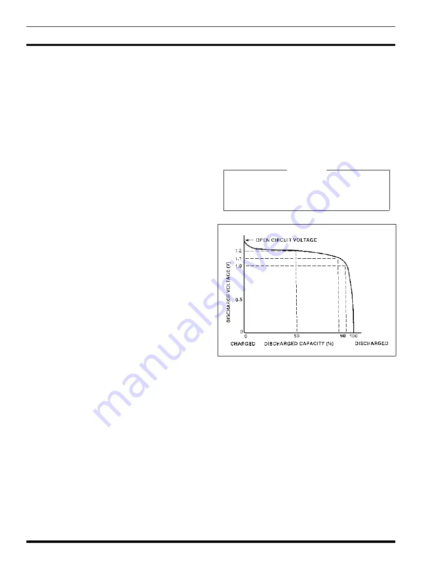
Discharge the battery pack at a normal discharge rate
until the output voltage is approximately 1 Volt per cell.
This equals 6 Volts output for the battery packs. Refer
to Figure 14. Note the flatness of the discharge curve
from 0% - 90%. Experience shows discharging below
the "knee" is not necessary.

2.

Complete a full charge cycle using an Ericsson GE
charger.

3.

Repeat steps 1 and 2. Performing this deep cycle at least
twice should be sufficient to restore battery pack capac-
ity.

RECHARGEABLE BATTERY 
PACK DISPOSAL

Under specific state laws, it may be illegal to dispose of

rechargeable batteries, rechargeable batteries packs and/or
products powered by rechargeable batteries except in accord-
ance with specific procedures. Special collection systems are
in place in certain states. Call Toll Free 1-800-822-9363 for
specific procedures for returning rechargeable batteries in
your state.

NOTE

This procedure is easily completed using Discharge
Analyzer 19B801506P9 and Rapid Multi-Charger
19B801506P16 or P18.

Figure 14 - Typical Cell Discharge Curve

LBI-38632

28

Summary of Contents for EDACS MTL

Page 1: ...h tested thoroughly in conventional mode This allows the technician using standard test equipment to verify the majority of the radio s circuitry is functional Any necessary repairs can be completed and the radio can then be tested in TABLE OF CONTENTS Page INTRODUCTION 1 TEST EQUIPMENT 2 FRONT COVER TEST ACCESSORY KIT 2 FUNCTIONAL TEST 3 DISASSEMBLY REASSEMBLY 3 ALIGNMENT PROCEDURES 6 SET UP PROC...

Page 2: ...62P4 Control Board Extender ST3559P2 RF Antenna Adapter top jack to BNC female TQ 0609 Test Box simulates all external UDC options 19B219079P1 Alignment Tool 0 1 slotted metal tips 19B801640P1 Alignment Tool 0 1 slotted tips In addition to the above listed equipment access to a local trunked site and a second EDACS portable or mobile radio will be necessary to test trunked mode operation PROGRAMMI...

Page 3: ...MBLY In the event internal service is required disassemble the radio in accordance with the following outlined steps See Figures 1 5 Reassemble the unit by following the steps in reverse order Observe screw lengths and do not over tighten the screws when reassemblingthe unit Torque specificationsare listed in Table 1 TOOLS REQUIRED TORX T6 Driver M1 5 Hex Driver or Wrench Needle Nose Pliers Small ...

Page 4: ...Control Board can now be removed Note the battery power and ground connections at the bottom of the board where the screws have been re moved SPEAKER MICROPHONE AND FLEX CIRCUIT ACCESS Remove the Control Board as previously stated and then remove the six 6 Torx screws that secure the die cast shield Remove the die cast shield by lifting the top end first and sliding it towards the top of the radio...

Page 5: ...h a spanner wrench remove the nuts securing the volume and channel controls and carefully slide the controls inside the radio Unscrew the two 2 screws G and GG and remove the J10 P10 Zebra strip securing plate HH See Figure 5 The Keypad Flex is now free for removal Additional screws J and JJ secure the LCD Board used with the M PA series radios Later Front Cover Assembly Keypad Flex Removal To rem...

Page 6: ...Extender cable between the RF Board and the Control Board See Figure 6 2 Slide the Dummy Battery onto the Front Cover Assem bly and connect the audio output leads to the distortion analyzer Place the Dummy Battery s on off switch in the OFF position to direct the speaker audio to its speak ers leads and to the distortion analyzer Connect the PC Programmer to the UDC 3 Set the power supply to 7 5 0...

Page 7: ...ror of less than 100 Hz SERVICE NOTES Throughout the service procedures presented in this manual the following information should be ob served The bench power supply should be set for 7 5 0 1 Vdc unless otherwise noted during trou bleshooting procedures presented in this man ual If a battery pack is used it should be fully charged Typical battery pack voltage will be 7 5 Vdc 20 over its full disch...

Page 8: ...15 513723 2 9 Vdc low 824 000000 1236 823 998764 824 001236 4 2 Vdc low 851 012500 1277 851 011223 851 013777 1 9 Vdc high 860 512500 1291 860 511209 860 513791 3 1 Vdc high 869 000000 1304 868 998696 869 001304 4 2 Vdc high Table 3 Maximum Transmitter Frequency Errors And Typical VCO TP2 TX Tuning Voltages Based on specified 1 5 ppm over the entire operating temperature range LBI 38632 8 ...
Page 9: ...mation can be used to check and align the receiver circuits Successful completion of these alignment procedures will verify a near 100 operating synthesizer and receiver stages 2nd Local Oscillator 1 Check the Reference Oscillator alignment as outlined in the TRANSMITTER ALIGNMENT section 2 Channel the unit to 860 5125 MHz 3 Set the RF signal generator to 860 5125 MHz 20 dBm and no modulation Appl...

Page 10: ...a of memory along with the associated channel information Changing the Tracking Data in the radio will not alter Chan nel Data of previously programmed channels Tracking Data should not normally be altered however it may be necessary to reprogram some of the values after aligning circuitry or replacing modules or other components which obsolete the previously programmed values Settings for each pa...

Page 11: ...1 and Exciter U9 for a gain problem Also check the VCO and Q6 for low RF drive Buffer Q6 supplies approximately 0 dBm to U9 Exciter U9 has an approximate gain of 23 dB and PAU1 has an approxi mate gain of 16 dB 5 Check Tracking and Channel Data Reprogram if neces sary Excessive Power Output Short battery life and possible damage to the PA module may result if this problem occurs in the power contr...

Page 12: ...re on Control Board Receiver inoperative or weak 1 Squelch levels programmed too high Press Monitor Button to disable squelch 2 Channel Guard or Type 99 Enabled See Operator s Manual 3 Defective antenna 4 RF Board problem Troubleshoot Rear Cover Assembly Transmitter inoperative or low 1 Power levels programmed low Check RF output and reprogram range unit if necessary 2 Weak battery 3 Defective ant...

Page 13: ...nd or noise With an RF input modulated at 1 kHz 3 kHz deviation RX AUDIO should be 100 150 mV rms approximately 350 mV p p If the 1 kHz audio is present troubleshoot the audio circuits in the Front Cover Assembly Noise levels on RX AUDIO with no RF input should be approximately 700 mV p p 3 Check for 7 5 Vdc at RF Amp U10 pin 5 and IF Amp U11 pin 1 Check U14 pin 7 for 5 8 Vdc 0 2 Vdc from A1 pin 1...

Page 14: ...equency counter with a high impedance probe or amp check TP8 for the 13 2 MHz 20 Hz at room temperature signal from Reference Oscillator U4 Re place U4 if this signal is not present and pin 1 is 5 4 Vdc Also verify the signal is present on U3 pin 2 See ALIGNMENT PROCEDURES for oscillator align ment details 5 Verify BAND SWITCH J102 pin 3 is at the correct logic level It should be low for transmit ...

Page 15: ...oltage From PLL Filter A1 TP3 45 0125 MHz IF Input To Receiver Back End U14 TP4 45 0125 MHz Output From IF Filter FLB1 TP5 45 0125 MHz Input To IF Filter FLB1 TP6 Band Switch Input To VCO High TX 806 825 MHz Low TX 851 870 MHz High RX 851 870 MHz TP7 LO Injection To Mixer U7 TP8 13 2 MHz Output From Reference Oscil lator U4 LBI 38632 15 ...

Page 16: ...ions screw mount ing points located on the bottom of the Control Board If dc power is not present at this point suspect fuse F1 or the battery plate connections Voltage regulators forthe Front Cover Assemblycircuits are the 5 0 Vdc 5V and the 5 4 Vdc V1 sources The RF 5 4 Vdc supply RF5 4 delivers dc power to the RF Board only Supply outputs can be tested at collector center termi nal of the assoc...

Page 17: ... NOTE Use an oscillo scope with a x10 probe or a frequency counter that has a high input impedance at least 10M ohms OS1 is the 2 00 MHz clock for the I O Microcontroller Replace Y4 if this clock frequency is in error Suspect Y4 or U18 if no signal is present Generally if the crystal is defective open 2 5 Vdc will be present at OS1 and no signal will be present Check TP1 OSCOUT for an 11 059 MHz c...

Page 18: ...ro to the I O Micro are primarily commands which cause the I O Micro to execute a commanded function Some examples include power up status Keypad Flex scan Audio Processor A D converter write read synthesizer load and tone generation All Personality to I O Micro message transfers are initiated by a low pulse on the UPCNTRL Message transfers from the I O Micro to the Personality Micro include statu...

Page 19: ...ignal points to an open series resistor on the Control Board or a defective output from U18 NOTE Temporarily connect LOCK J102 P2 pin 8 to ground to view these waveforms 4 Verify BAND SWITCH J102 P2 pin 3 is at the correct logic level It should be low for transmit frequencies of 806 825 MHz and high for transmit frequencies of 851 870 MHz BAND SWITCH should remain low for all receive frequencies T...

Page 20: ... the UDC Flex or op amp U19 1 Connect an external microphone and check the audio level at J1 pin 12 Average speech in the microphone should produce 10 30 mV rms here Signal on U19 1 pin 1 BUFINTMIC should be 7 to 10 times greater than EXT MIC HI Complete Mic Audio Failure If both the external and internal microphones are not functioning apply an ac coupled 110 mV rms 1 kHz tone to the UDC EXT MIC ...

Page 21: ...se levels STRONG RF SIGNAL no modulation J101 P1 pin 4 700 mV p p 0 V p p U8 pin 8 2100 mV p p 0 V p p U7 pin 3 650 mV p p 0 V p p U7 pin 56 3 2 Vdc 2 7 Vdc U7 pin 55 3 5 Vdc 2 7 Vdc Table 10 Typical Receiver Audio Levels At Full Volume TEST LOCATION LEVEL mV p p COMMENT J101 P1 pin 4 300 RX Output RXDISCOUT U8 pin 8 900 RX Buffer Output BUFDISC U7 pin 18 450 Audio Processor Output U7 pin 19 120 A...

Page 22: ...emoved With the Front Cover face down on the bench apply audio from a signal generator to the second and third pins from the left The speaker impedance is 24 ohms and it is a 1 2 Watt device Receive Channel Guard Or Trunked Low Speed Data Problems Decode Mode Filtering and limiting of Channel Guard and trunked low speed data occurs in Audio Processor U7 A Channel Guard signal is decoded by I O Mic...

Page 23: ...or 9600 baud pulses when a trunk call is attempted Signal level should be 3 Vp p with rise and fall times 100 micro seconds If no pulses are present there is a communica tion problem between U4 and U5 or U5 is defective 2 Check U14 pin 9 It should be high for 800 MHz EDACS applications 3 Stage U6 1 and associated RC networks filter or round the digital pulses to a signal which can modulate the FM ...

Page 24: ...d on the PWB Use as little solder as possible 2 Place the component on the PWB pads observing proper orientation for capacitors diodes transistors etc 3 Simultaneously touch the tinned terminal end and the tinned pad with the soldering iron Slightly press the component down on the board as the solder is liquefied Solder all terminals allowing the component time to cool between each application of ...

Page 25: ...U18 TP1 11 0592 MHz Clock From Modem U5 OSCOUT TP2 Reset Output From Modem U5 TP3 5 0 Vdc Regulated Supply 5V TP4 Reset Comparator Output VCB TP5 DTMF Tones TP6 2 7 Vdc Reference Supply VCC 2 TP7 8 MHz Clock Output From Audio Processor U7 TP8 Internal Mic Amp Output BUFINTMIC TP8 External Mic Amp Output BUFEXTMIC LBI 38632 25 ...

Page 26: ...gh holes and clean all flux from the board Next install the replacement module making sure that all pins align in the proper holes Resolder the pins to the board Clean the flux from the board using an approved solvent Clip any excess lead length INTERNAL LITHIUM BATTERY REPLACEMENT All personality data is stored in RAM IC U1 on the Control Board This data includes TX and RX operating frequencies C...

Page 27: ...ese seals When installing a new seal make sure it is seated properly before reassembly BATTERY PACKS Battery packs available for use with the radio include high and extra high capacity rechargeable units All of the rechargeable battery packs are factory sealed and are not field serviceable other than properly charging them and cleaning the contacts Figure 13 outlines a typical battery pack Figure ...

Page 28: ...NDITION Rechargeable batteries can develop a condition of re duced capacity sometimes called Memory Effect This condition can occur when a battery is continuously charged for long periods of time or when a regularly performed duty cycle allows the battery to expend only a limited portion of its capacity If the battery pack is seldom used and left on a continu ous charge for long periods it may dev...

Page 29: ...ch personality programming STOP PLATE REPOSITIONING 1 Remove the Control Knob using an M1 5 hex wrench 2 Lift the stop plate using small needle nose pliers 3 Reposition the stop plate by aligning the raised bar to the channel marking one 1 number higher than the number of positions required For example if eight 8 unique positions are required align the raised bar to the 9 If sixteen 16 positions a...

Page 30: ...LBI 38632 RF BOARD MODULE AND IC DATA A1 PLL FILTER REGULATOR 19C852056G1 19C852057 Sh 1 Rev 1 19C852056 Sh 1 Rev 0 30 ...

Page 31: ...RF BOARD MODULE AND IC DATA LBI 38632 A2 POWER CONTROLLER 19C851922G1 19C851922 Rev 2 19C851920 Rev 0 31 ...

Page 32: ...LBI 38632 RF BOARD MODULE AND IC DATA FLA1 FLA2 RF BANDPASS FILTER 19A704888P1 FLB1 IF MONOLITHIC CRYSTAL FILTER 19A705328P5 U1 806 870 MHz POWER AMPLIFIER 19A705962P1 32 ...

Page 33: ...RF BOARD MODULE AND IC DATA LBI 38632 U2 ANTENNA T R SWITCH 19A149809P1 U3 SYNTHESIZER 19B800902P4 U4 13 2 MHz REFERENCE OSCILLATOR 19B235948G1 33 ...

Page 34: ...LBI 38632 RF BOARD MODULE AND IC DATA U5 LOW PASS FILTER 19A149810P1 U7 800 MHz MIXER 19A705706P3 34 ...

Page 35: ...RF BOARD MODULE AND IC DATA LBI 38632 U8 PRESCALER 19A705985P1 U9 800 MHz EXCITER 19C851848G1 19C337499 Rev 0 35 ...

Page 36: ...LBI 38632 RF BOARD MODULE AND IC DATA U10 800 MHz RF AMPLIFIER 19C851857G1 U11 45 0125 MHz IF AMPLIFIER 19C336876G1 19C337062 Rev 2 19C851859 Rev 0 36 ...

Page 37: ...RF BOARD MODULE AND IC DATA LBI 38632 U14 RECEIVER BACK END 19B801642G1 Y2 VCO earlier 19B235947G1 19C337500 Rev 2 37 ...

Page 38: ...LBI 38632 RF BOARD MODULE AND IC DATA Y4 VCO later 19C852149G1 19C852149 Sh 1 Rev 6 19C852147 Sh 1 Rev 0 38 ...

Page 39: ...CONTROL BOARD IC DATA LBI 38632 CR5 2 5 VOLT REFERENCE 19A149634P1 U1 8K x 8 BIT STATIC RAM 19A705603P7 39 ...

Page 40: ...LBI 38632 CONTROL BOARD IC DATA U2 64K x 8 BIT EPROM 19A705963P2 U3 TRI STATE TRANSCEIVER 19A703741P118 40 ...

Page 41: ...CONTROL BOARD IC DATA LBI 38632 U4 8 BIT MICROPROCESSOR 19A705557P3 U5 MODEM 19A704727P5 41 ...

Page 42: ...LBI 38632 CONTROL BOARD IC DATA U6 U8 QUAD OP AMP 19A702293P1 U7 AUDIO PROCESSOR 19A705851P1 42 ...

Page 43: ...CONTROL BOARD IC DATA LBI 38632 U9 DUAL AND OR GATE 19A703483P113 U10 AUDIO AMPLIFIER 19A705452P2 U11 HEX INVERTER 19A703483P304 43 ...

Page 44: ...LBI 38632 CONTROL BOARD IC DATA U12 U19 DUAL OP AMP 19A702293P2 U14 QUAD MULTIPLEXER 19A700029P633 U17 QUAD COMPARATOR 19A704125P1 44 ...

Page 45: ...CONTROL BOARD IC DATA LBI 38632 U18 MICROCONTROLLER 19A149861 45 ...

Page 46: ...LBI 38632 KEYPAD FLEX IC DATA U1 8 BIT SHIFT REGISTER 19A704423P2 U2 8 BIT LATCHING SHIFT REGISTER 19A704423P3 46 ...

Reviews: