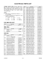
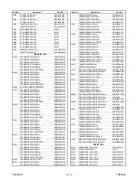
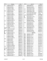

20030807
3-3-11
TD900EL
C2218
CERAMIC CAP.(AX) F Z 0.022
µ
F/25V
CCA1EZTFZ223
C2222
CERAMIC CAP.(AX) B K 100pF/50V
CCA1JKT0B101
C2224
ELECTROLYTIC CAP. 47
µ
F/25V M or
CE1EMASDL470
ELECTROLYTIC CAP. 47
µ
F/25V M
CE1EMASTL470
C2225
ELECTROLYTIC CAP. 4.7
µ
F/50V M or
CE1JMASDL4R7
ELECTROLYTIC CAP. 4.7
µ
F/50V M
CE1JMASTL4R7
C2226
ELECTROLYTIC CAP. 4.7
µ
F/50V M or
CE1JMASDL4R7
ELECTROLYTIC CAP. 4.7
µ
F/50V M
CE1JMASTL4R7
C2228
ELECTROLYTIC CAP. 10
µ
F/50V M or
CE1JMASDL100
ELECTROLYTIC CAP. 10
µ
F/50V M
CE1JMASTL100
C2229
ELECTROLYTIC CAP. 10
µ
F/50V M or
CE1JMASDL100
ELECTROLYTIC CAP. 10
µ
F/50V M
CE1JMASTL100
C2230
ELECTROLYTIC CAP. 10
µ
F/50V M or
CE1JMASDL100
ELECTROLYTIC CAP. 10
µ
F/50V M
CE1JMASTL100
C2231
CERAMIC CAP.(AX) SL J 47pF/50V
CCA1JJTSL470
C2232
CERAMIC CAP.(AX) SL J 47pF/50V
CCA1JJTSL470
C2233
CERAMIC CAP.(AX) B K 220pF/50V
CCA1JKT0B221
C2236
CERAMIC CAP.(AX) CH J 20pF/50V
CCA1JJTCH200
C2238
CERAMIC CAP.(AX) B K 220pF/50V
CCA1JKT0B221
C2239
ELECTROLYTIC CAP. 10
µ
F/50V M or
CE1JMASDL100
ELECTROLYTIC CAP. 10
µ
F/50V M
CE1JMASTL100
C2261
ELECTROLYTIC CAP. 47
µ
F/25V M or
CE1EMASDL470
ELECTROLYTIC CAP. 47
µ
F/25V M
CE1EMASTL470
C2262
ELECTROLYTIC CAP. 47
µ
F/25V M or
CE1EMASDL470
ELECTROLYTIC CAP. 47
µ
F/25V M
CE1EMASTL470
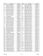
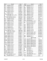
C2301
CERAMIC CAP.(AX) B K 1000pF/50V
CCA1JKT0B102
C2303
CERAMIC CAP.(AX) F Z 0.022
µ
F/25V
CCA1EZTFZ223
C2304
CERAMIC CAP.(AX) SL J 68pF/50V
CCA1JJTSL680
C2401
ELECTROLYTIC CAP. 47
µ
F/25V M or
CE1EMASDL470
ELECTROLYTIC CAP. 47
µ
F/25V M
CE1EMASTL470
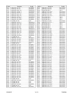
C2416
ELECTROLYTIC CAP. 470
µ
F/16V M or
CE1CMASDL471
ELECTROLYTIC CAP. 470
µ
F/16V M
CE1CMASTL471
C2418
ELECTROLYTIC CAP. 470
µ
F/6.3V M or
CE0KMASDL471
ELECTROLYTIC CAP. 470
µ
F/6.3V M
CE0KMASTL471
C2423
CERAMIC CAP.(AX) X M 2200pF/16V
CCA1CMT0X222
C2429
ELECTROLYTIC CAP. 220
µ
F/6.3V M or
CE0KMASDL221
ELECTROLYTIC CAP. 220
µ
F/6.3V M
CE0KMASTL221
C2432
CERAMIC CAP.(AX) B K 100pF/50V
CCA1JKT0B101
C2604
ELECTROLYTIC CAP. 470
µ
F/6.3V M or
CE0KMASDL471
ELECTROLYTIC CAP. 470
µ
F/6.3V M
CE0KMASTL471
C2605
#
METALLIZED FILM CAP. 0.1
µ
F/250V or
CT2E104MS037
#
FILM CAP.(MP) 0.1
µ
F/250V K or
CT2E104DC011
#
METALLIZED FILM CAP. 0.1
µ
F/275V K
CT2E104HJE06
C2606
CERAMIC CAP. F Z 0.01
µ
F/500V or
CCD2JZP0F103
CERAMIC CAP. 0.01
µ
F/AC250V or
CCD2EZA0F103
CERAMIC CAP. E Z 0.01
µ
F/500V
CCD2JZP0E103
C2607
CERAMIC CAP. F Z 0.01
µ
F/500V or
CCD2JZP0F103
CERAMIC CAP. 0.01
µ
F/AC250V or
CCD2EZA0F103
CERAMIC CAP. E Z 0.01
µ
F/500V
CCD2JZP0E103
C2610
ELECTROLYTIC CAP. 470
µ
F/200V or
CA2D471NC013
ELECTROLYTIC CAP. 470
µ
F/200V M W/F
CA2D471EA029
C2611
CERAMIC CAP. BN 820pF/2KV or
CCD3DKA0B821
CERAMIC CAP. 820pF/2KV or
CA3D821PAN04
CERAMIC CAP RB 820pF/2KV
CA3D821TE006
C2612
FILM CAP.(P) 0.033
µ
F/50V J or
CMA1JJS00333
FILM CAP.(P) 0.033
µ
F/50V J
CA1J333MS029
C2613
FILM CAP.(P) 0.0012
µ
F/50V J or
CMA1JJS00122
FILM CAP.(P) 0.0012
µ
F/50V J
CA1J122MS029
C2614
#
FILM CAP.(P) 0.082
µ
F/50V J or
CMA1JJS00823
#
FILM CAP.(P) 0.082
µ
F/50V J
CA1J823MS029
C2615
CERAMIC CAP. BN 820pF/2KV or
CCD3DKA0B821
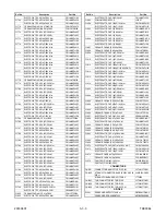
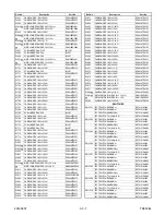
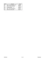
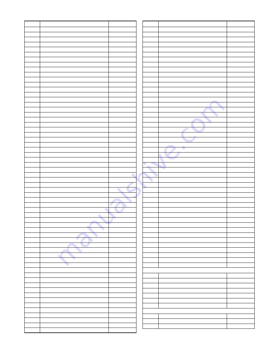
Ref. No.
Description
Part No.
CERAMIC CAP. 820pF/2KV or
CA3D821PAN04
CERAMIC CAP RB 820pF/2KV
CA3D821TE006
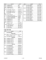
C2616
ELECTROLYTIC CAP. 100
µ
F/160V M or
CE2CMZPDL101
ELECTROLYTIC CAP. 100
µ
F/160V M or
CE2CMZPTL101
ELECTROLYTIC CAP. 100
µ
F/160V M W/F
CE2CMZNTL101
C2617
ELECTROLYTIC CAP. 470
µ
F/35V M or
CE1GMASDL471
ELECTROLYTIC CAP. 470
µ
F/35V M
CE1GMASTL471
C2618
ELECTROLYTIC CAP. 1000
µ
F/16V M or
CE1CMZPDL102
ELECTROLYTIC CAP. 1000
µ
F/16V M(VR/HC)
CE1CMZNTL102
C2619
ELECTROLYTIC CAP. 1000
µ
F/16V M or
CE1CMZPDL102
ELECTROLYTIC CAP. 1000
µ
F/16V M(VR/HC)
CE1CMZNTL102
C2620
ELECTROLYTIC CAP. 1000
µ
F/16V M or
CE1CMZPDL102
ELECTROLYTIC CAP. 1000
µ
F/16V M(VR/HC)
CE1CMZNTL102
C2621
ELECTROLYTIC CAP. 100
µ
F/16V M or
CE1CMASDL101
ELECTROLYTIC CAP. 100
µ
F/16V M
CE1CMASTL101
C2622
FILM CAP.(P) 0.0047
µ
F/50V J or
CMA1JJS00472
FILM CAP.(P) 0.0047
µ
F/50V J
CA1J472MS029
C2624
CERAMIC CAP.(AX) B K 0.01
µ
F/50V
CCA1JKT0B103
C2625
ELECTROLYTIC CAP. 0.47
µ
F/50V M or
CE1JMASDLR47
ELECTROLYTIC CAP. 0.47
µ
F/50V M
CE1JMASTLR47
C2626
ELECTROLYTIC CAP. 10
µ
F/50V M or
CE1JMASDL100
ELECTROLYTIC CAP. 10
µ
F/50V M
CE1JMASTL100
C2630
SAFETY CAP. 4700pF/250V KX
CA2E472MR050
C2631
ELECTROLYTIC CAP. 1000
µ
F/6.3V M or
CE0KMASDL102
ELECTROLYTIC CAP. 1000
µ
F/6.3V M
CE0KMASTL102
C2632
ELECTROLYTIC CAP. 100
µ
F/16V M or
CE1CMASDL101
ELECTROLYTIC CAP. 100
µ
F/16V M
CE1CMASTL101
C2633
ELECTROLYTIC CAP. 47
µ
F/25V M or
CE1EMASDL470
ELECTROLYTIC CAP. 47
µ
F/25V M
CE1EMASTL470
C2637
ELECTROLYTIC CAP. 470
µ
F/6.3V M or
CE0KMASDL471
ELECTROLYTIC CAP. 470
µ
F/6.3V M
CE0KMASTL471
C2640
ELECTROLYTIC CAP. 470
µ
F/16V M or
CE1CMASDL471
ELECTROLYTIC CAP. 470
µ
F/16V M
CE1CMASTL471
C2642
CERAMIC CAP.(AX) B K 1000pF/50V
CCA1JKT0B102
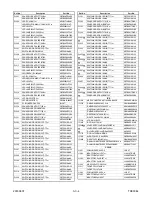
C2643
ELECTROLYTIC CAP. 470
µ
F/10V M or
CE1AMASDL471
ELECTROLYTIC CAP. 470
µ
F/10V M
CE1AMASTL471
C2645
CERAMIC CAP.(AX) B K 0.01
µ
F/50V
CCA1JKT0B103
C2646
ELECTROLYTIC CAP. 2200
µ
F/6.3V M or
CE0KMZPDL222
ELECTROLYTIC CAP. 2200
µ
F/6.3V M
CE0KMZNTL222
C2647
ELECTROLYTIC CAP. 470
µ
F/16V M or
CE1CMASDL471
ELECTROLYTIC CAP. 470
µ
F/16V M
CE1CMASTL471
C2650
CERAMIC CAP.(AX) B K 2200pF/50V
CA1J222TU011
C2651
CERAMIC CAP.(AX) B K 2200pF/50V
CA1J222TU011
C2661
ELECTROLYTIC CAP. 100
µ
F/16V M or
CE1CMASDL101
ELECTROLYTIC CAP. 100
µ
F/16V M
CE1CMASTL101
C2662
CERAMIC CAP.(AX) B K 1000pF/50V
CCA1JKT0B102
C2671
CERAMIC CAP. B K 2200pF/500V or
CCD2JKP0B222
CERAMIC CAP. B K 2200pF/500V
CCD2JKS0B222
CONNECTORS
CN2401
FMN CONNECTOR, TOP 12P 12FMN-BTRK
JCFNG12JG002
CN2402
FMN CONNECTOR, TOP 22P 22FMN-BTRK
JCFNG22JG002
CN2601
CONNECTOR BASE, 2P TV-50P-02-V3 or
J3TVC02TG002
CONNECTOR BASE, 2P RTB-1.5-2P
J3RTC02JG001
CN2602
CONNECTOR BASE, 6P TUC-P06P-B1
J3TUA06TG001
CN2803
TWG CONNECTOR 19P TWG-P19P-A1
J3TWA19TG001
CN2804
TWG CONNECTOR 19P TWG-P19P-A1
J3TWA19TG001
DIODES
D2206
ZENER DIODE MTZJT-776.2B or
QDTB0MTZJ6R2
ZENER DIODE DZ-6.2BSBT265
NDTB0DZ6R2BS
D2245
PCB JUMPER D0.6-P5.0
JW5.0T
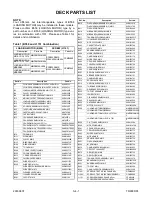
Ref. No.
Description
Part No.
Summary of Contents for EC720E
Page 2: ...EC720E T1008UJ 2004 06 22 ...
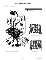
Page 22: ...1 7 4 TD900DC S 4 S 4 S 4 S 4 4 CRT Anode Cap CRT CBA Fig 3 ...
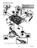
Page 93: ...2 4 8 TD951DA Fig DM16 41 42 43 L 13 44 45 P 9 Slide Fig DM17 ...
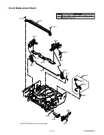
Page 97: ...3 1 3 TD900PEX S4 S1 X1 TAPE X5 X4 X2 X3 S3 S6 S7 S2 PACKING TAPE Packing ...
Page 119: ...Printed in Japan 2003 08 25 HO 6720FDD TD900UA ...


