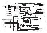
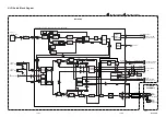
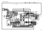
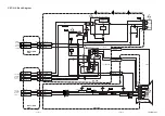
background image

1-8-3

TD900EA

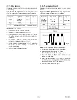
4. V. Size Adjustment

Purpose: To obtain correct vertical height of screen
image.

Symptom of Misadjustment: If V. Size is incorrect,
vertical height of image on the screen may not be
properly displayed.

1. Enter the Service mode. (See page 1-8-1.) 

Press "9" button on the remote control unit and
select V-S Mode. (Press "9" button then display will
change to V-P and V-S).

2. Input monoscope pattern.

3. Press CH 

o

 / 

p

 buttons on the remote control unit

so that the monoscope pattern is 90

±

5% of display

size and the circle is round.

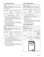
5. V. Shift Adjustment

Purpose: To obtain correct vertical position of screen
image.

Symptom of Misadjustment: If V. position is incor-
rect, vertical position of image on the screen may not
be properly displayed.

1. Enter the Service mode. (See page 1-8-1.) 

Press "9" button on the remote control unit and
select V-P Mode. (Press "9" button then display will
change to V-P and V-S).

2. Input monoscope pattern.

3. Press CH 

o

 / 

p

 buttons on the remote control unit

so that the top and bottom of the monoscope pat-
tern are equal to each other.

6. H. Shift Adjustment

Purpose: To obtain correct horizontal position and
size of screen image.

Symptom of Misadjustment: Horizontal position and
size of screen image may not be properly displayed.

1. Enter the Service mode. (See page 1-8-1.) 

Press "8" button on the remote control unit and
select H-P Mode. 

2. Input monoscope pattern.

3. Press CH 

o

 / 

p

 buttons on the remote control unit

so that the left and right side of the monoscope pat-
tern are equal to each other.

4. Turn the power off and on again.

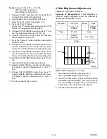
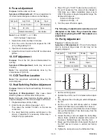
7. Cut-off Adjustment

Purpose: To adjust the beam current of R, G, B, and
screen voltage.

Symptom of Misadjustment: White color may be
reddish, greenish or bluish.

Test point

Adj. Point

Mode

Input

---

CH 

o

 / 

p  

buttons

---

Monoscope

Tape

M. EQ.

Spec.

---

Pattern Generator

90

±

5%

Test point

Adj. Point

Mode

Input

---

CH 

o

 / 

p  

buttons

---

Monoscope

Tape

M. EQ.

Spec.

---

Pattern Generator

---

Test point

Adj. Point

Mode

Input

---

CH 

o

 / 

p  

buttons

---

Monoscope

Tape

M. EQ.

Spec.

---

Pattern Generator

---

Test point

Adj. Point

Mode

Input

---

Screen-Control

Ext.

Black 

Raster / 

White 

Raster

Tape

M. EQ.

Spec.

---

Pattern Generator

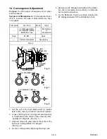
See Reference 

Notes below

Figure

PATTERN GENERATOR

RF INPUT

Fig. 3

Summary of Contents for EC720E

Page 1: ...ASSETTE DOOR T1008UJ 1EM420198 A1 7 TRAY PANEL T1008UJ 1EM420197 A3 RATING LABEL T1008UJ A4 Not Used S1 CARTON T1008UJ 1EM420196 X2 OWNER S MANUAL T1008UJ 1EMN20069 X3 REMOTE CONTROL NE230UD 151 ECNX501 NE230UD NE230UD X5 SHEET RETURN STOP T5510UL 1EM420161 SERVICE MANUAL SUPPLEMENT This service manual shows only the differences between the model EC720E and the original model 6720FDE All other inf...

Page 2: ...EC720E T1008UJ 2004 06 22 ...

Page 3: ...icing I Adjustment Procedures I Schematic Diagrams I CBA s Sec 2 Deck Mechanism Section I Standard Maintenance I Alignment for Mechanism I Disassembly Assembly of Mechanism Sec 3 Exploded views and Parts List Section I Exploded views I Parts List 20 COLOR TV DVD VCR 6720FDD ...

Page 4: ...roper ser vice methods may damage the equipment It also is important to understand that these CAUTIONS and NOTICES ARE NOT EXHAUSTIVE Funai could not possibly know evaluate and advice the service trade of all conceivable ways in which service might be done or of the possible hazardous consequences of each way Consequently Funai has not undertaken any such broad evalua tion Accordingly a servicer w...

Page 5: ...tions 1 6 1 Cabinet Disassembly Instructions 1 7 1 Electrical Adjustment Instructions 1 8 1 FIRMWARE Renewal Mode 1 9 1 Block Diagrams 1 10 1 Schematic Diagrams CBA s and Test Points 1 11 1 Waveforms 1 12 1 Wiring Diagrams 1 13 1 System Control Timing Charts 1 14 1 IC Pin Function Descriptions 1 15 1 Lead Identifications 1 16 1 Sec 1 Main Section I Specifications I Preparation for Servicing I Adju...

Page 6: ...ide m m 1 5 2 Tint Control Range deg 30 3 Contrast Control Range dB 6 2 4 Brightness 100 White Full Field Contrast Max ft L 35 24 5 Color Temperature K 9200 Description Condition Unit Nominal Limit 1 Horizontal Resolution TDV 540 TIT 2 CHP 16 Line 330 320 2 Video S N at CN3400 TDV 540 TIT 2 CHP 6 dB 60 55 3 S N Chroma at CN3400 AM dB 58 53 TDV 540 TIT 2 CHP 17 PM dB 58 53 4 Audio Distortion LPCM 4...

Page 7: ...al Limit 1 Horizontal Resolution R P SP Line 230 200 2 Jitter Low R P SP µS 0 1 0 2 3 S N Chroma AM SP R P SP dB 38 33 PM SP R P SP dB 38 33 4 Wow Flutter JIS UNWTD R P SP 0 25 0 5 Description Condition Unit Nominal Limit 1 Video S N 80dBµV TV4ch dB 45 40 2 Audio S N W LPF dB 45 40 Description Condition Unit Nominal Limit 1 Audio Output Power R P SP W 1 0 0 8 2 Audio S N W LPF R P SP dB 40 36 3 Au...

Page 8: ...tion shown in the figure When checking the laser diode be sure to keep your eyes at least 30cm away from the pickup lens when the diode is turned on Do not look directly at the laser beam Caution Use of controls and adjustments or doing procedures other than those specified herein may result in hazardous radiation exposure Do not look directly at the laser beam coming from the pickup or allow it t...

Page 9: ...rongs tied together and touch the other ohmme ter lead in turn to each tuner antenna input ex posed terminal screw and if applicable to the coaxial connector If the measured resistance is less than 1 0 megohm or greater than 5 2 mego hm an abnormality exists that must be corrected before the instrument is returned to the customer Repeat this test with the instrument AC switch in the off position d...

Page 10: ...ted to the ground side of the AC power source To confirm that the AC power plug is inserted correctly with an AC volt meter measure between the chassis and a known earth ground If a voltage reading in excess of 1 0V is obtained remove and reinsert the AC power plug in the opposite polarity and again measure the voltage potential between the chassis and a known earth ground b Some TV receiver chass...

Page 11: ...not contact sharp edged or pointed parts H When a power cord has been replaced check that 5 6 kg of force in any direction will not loosen it I Also check areas surrounding repaired locations J Be careful that foreign objects screws solder droplets etc do not remain inside the set K Crimp type wire connector When replacing the power transformer in sets where the connections between the power cord ...

Page 12: ...er cord plug prongs and externally exposed accessible parts RF terminals antenna terminals video and audio input and output terminals microphone jacks earphone jacks etc Measuring Method Power ON Insert load Z between B earth ground power cord plug prongs and exposed accessible parts Use an AC voltmeter to measure across both terminals of load Z See Fig 2 and following table Table 2 Leakage curren...

Page 13: ...r With Soldering Iron a Using desoldering braid remove the solder from all pins of the Flat Pack IC When you use solder flux which is applied to all pins of the Flat Pack IC you can remove it easily Fig S 1 3 b Lift each lead of the Flat Pack IC upward one by one using a sharp pin or wire to which solder will not adhere iron wire When heating the pins use a fine tip soldering iron or a hot air Des...

Page 14: ...older all pins of the Flat Pack IC Make sure that none of the pins have solder bridges Fig S 1 1 Hot air Flat Pack IC Desoldering Machine CBA Flat Pack IC Tweezers Masking Tape Fig S 1 2 Flat Pack IC Desoldering Braid Soldering Iron Fig S 1 3 Fine Tip Soldering Iron Sharp Pin Fig S 1 4 To Solid Mounting Point Soldering Iron Iron Wire or Hot Air Blower Fig S 1 5 Example Pin 1 of the Flat Pack IC is...

Page 15: ... static electricity that may be charged on the body Ground for Work Bench Be sure to place a conductive sheet or copper plate with proper grounding 1MΩ on the work bench or other surface where the semiconductors are to be placed Because the static electricity charge on the clothing will not escape through the body grounding band be careful to avoid contacting semiconductors to clothing Presolder C...

Page 16: ... mounted on the Main CBA When deck mechanism assembly is removed from the Main CBA due to servicing this switch can not be oper ated automatically Preparing 2 1 To eject the tape press the STOP EJECT button on the unit or Remote Control 2 When you want to record during the Service mode press the Rec button while depressing SW1211 REC SAFETY SW on the Main CBA Key Adjustment Mode MENU Picture adjus...

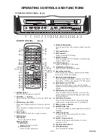
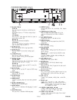
Page 17: ...one not supplied for personal listening 19 VIDEO input Jack Connect to the video output jack of a video camera or VCR 20 AUDIO L R input Jacks Connect to the audio output jacks of a video camera or VCR 21 Cassette compartment 22 PICTURE Button Press to adjust the picture REMOTE CONTROL Fig 2 1 POWER Button Press to turn the power on and off 2 VOLUME X Y Buttons Press to control the volume level fo...

Page 18: ...tton Repeats playback of the current disc title chapter or track 36 ANGLE Button DVD mode Press to change the camera angle to see the sequence being played back from a different angle 37 A B REPEAT Button Repeats playback of a selected section 38 RETURN Button Returns to the previous operation in the DVD setup mode 39 ENTER Button Press to accept a setting 40 Arrow Buttons TV VCR Mode Press to sel...

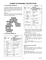
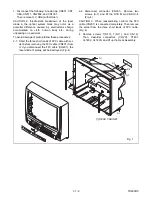
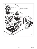
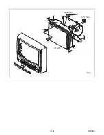
Page 19: ...Reference Notes in the Table Reference Notes in the Table Caution When removing the CRT be sure to discharge the Anode Lead of the CRT with the CRT Ground Wire before removing the Anode Cap Reference Notes in the Table CAUTION 1 Discharge the Anode Lead of the CRT with the CRT Ground Wire before removing the Anode Cap ID LOC No PART REMOVAL Fig No REMOVE UNHOOK UNLOCK RELEASE UNPLUG DESOLDER Note ...

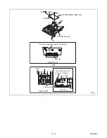
Page 20: ...Short the three short lands of FPC cable with sol der before removing the FFC cable CN201 from it If you disconnect the FFC cable CN201 the laser diode of pickup will be destroyed Fig 4 2 2 Disconnect connector CN301 Remove two screws S 7 and lift the DVD Main CBA Unit Fig 4 CAUTION 3 When reassembling confirm the FFC cable CN201 is connected completely Then remove the solder from the three short ...

Page 21: ... 10 S 10 S 10 S 8 S 13 S 8 S 6 S 6 S 6 S 5 S 5 S 5 S 13 S 11 S 12 S 8 5 Shield Box 6 DVD Mechanism Unit 8 Power Supply AV CBA 9 Function CBA 10 Deck Assembly 11 Main CBA 2 H V CBA wih Holder H V CBA 3 Tray Chassis Unit Fig 2 ...

Page 22: ...1 7 4 TD900DC S 4 S 4 S 4 S 4 4 CRT Anode Cap CRT CBA Fig 3 ...

Page 23: ... 4 View for B Pickup Unit C B Short the three short lands by soldering Short the three short lands by soldering FPC Cable Connector Slide DVD Mechanism 7 DVD Main CBA Unit View for C View for A OR A S 7 CN201 S 7 CN301 ...

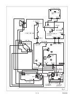
Page 24: ...SE ONLY DVD MAIN CBA FE HEAD CYLINDER ASSEMBLY AC HEAD ASSEMBLY CAPSTAN MOTOR DECK ASSEMBLY CN571 CL502A CL503A CL501A H V CBA TUNER CN1802 CL1201 CN1301 CN1803 CN1804 CN1805 CL1402 CL1401 CL1403 MAIN CBA CN2602 CN2401 CN2402 CN2804 CN2803 CN2601 POWER SUPPLY AV CBA CN2805 CN2801 CRT CBA TO SPEAKER TO SPEAKER ...

Page 25: ...e microproces sor with a jumper wire How to Set up the Service mode Service Mode 1 Use the service remote control unit 2 Turn the power on Use main power on the TV unit 3 To enter the TV mode press CH UP or CH DOWN button on the TV unit 4 Press DISC MENU button on the service remote control unit Version of micro computer will display on the CRT Ex 057 001 X Ray Protection Test X Ray protection tes...

Page 26: ...n again 3 C Trap Adjustment Purpose To get minimum leakage of the color signal carrier Symptom of Misadjustment If C Trap Adjustment is incorrect stripes will appear on the screen Note D1304 Cathode B Out Main CBA 1 Connect Oscilloscope to D1304 Cathode 2 Input a color bar signal from RF input Enter the Service mode See page 1 8 1 3 Press 0 button on the remote control unit and select C TRAP Mode ...

Page 27: ...hat the top and bottom of the monoscope pat tern are equal to each other 6 H Shift Adjustment Purpose To obtain correct horizontal position and size of screen image Symptom of Misadjustment Horizontal position and size of screen image may not be properly displayed 1 Enter the Service mode See page 1 8 1 Press 8 button on the remote control unit and select H P Mode 2 Input monoscope pattern 3 Press...

Page 28: ...rizontal line becomes white 10 Choose CUT OFF DRIVE mode then press 4 but ton 11 Input the White Raster Signal from Video In 12 Adjust the RED DRIVE as needed with the CH o p buttons to get the following value X 286 Y 294 13 Choose CUT OFF DRIVE mode then press 5 Adjust the BLUE DRIVE as needed with the CH o p buttons to get the following value X 286 Y 294 14 Turn the power off and on again 8 Sub ...

Page 29: ...e remote con trol unit if necessary The value will be changed in 0 5H steps up or down Adjustable range is up to 9 5H If the value is beyond adjustable range the display will change as Lower out of range 0 0H Upper out of range H 5 Turn the power off and on again The following 2 adjustments normally are not attempted in the field They should be done only when replacing the CRT then adjust as a pre...

Page 30: ...s at the center of the screen by rotating RB G C P Magnet See Fig 8 4 Fix the C P Magnets by tightening the Ring Lock 5 Remove the DY Wedges and slightly tilt the Deflec tion Yoke horizontally and vertically to obtain the best overall convergence 6 Fix the Deflection Yoke by carefully inserting the DY Wedges between CRT and Deflection Yoke Test point Adj Point Mode Input C P Magnet RB C P Magnet R...

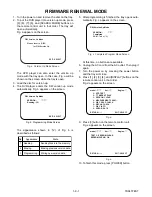
Page 31: ...let Then plug it again 7 Turn the power on by pressing the power button and the tray will close 8 Press 1 2 3 4 and DISPLAY buttons on the remote control unit in that order Fig d appears on the screen 9 Press 3 button on the remote control unit Fig e appears on the screen 10 To finish this mode press POWER button F W Version Up Mode Please insert a DISC for F W Version Up EXIT SELECT Fig a Version...

Page 32: ...TD900BLS SCL MEMORY SDA 6 5 P DOWN 84 P ON H P DOWN P ON H 31 LD SW 1 I 2 C OPEN 45 71 AL 5V SW1212 LD SW CS 7 FROM TO POWER SUPPLY BLOCK SDA SCL FROM TO CHROMA BLOCK IC1202 WF3 ENV DET 17 V H SW ENV DET V H SW 16 SDA SCL Hi Fi H SW ST SAP IN NORMAL H DVD MAIN POWER Hi Fi H SW 19 26 48 21 DVD H DVD A MUTE 42 5 KEY SWITCH SW1201 SW1203 SW1206 SW1210 5 5 KEY1 CN2805 CN2803 CN1805 KEY SWITCH SW2401 S...

Page 33: ...01 WF1 TP1403 HA MONITOR BUFFER DV SYNC SP LP SLP ROTA DV SYNC ROTA 14 36 16 71 39 59 73 SPL PLAY REC EE PB RENTAL SPL PLAY REC EE PB RENTAL 42 EXT H 74 45 47 49 44 Q1402 WF6 WF5 WF4 WF2 L R VIDEO R 1 HEAD VIDEO L 1 HEAD DECK ASSEMBLY V R 1 V COM V L 1 9 8 7 V L 2 V COM V R 2 6 5 4 13 88 89 90 91 FROM TO SERVO SYSTEM CONTROL BLOCK CYLINDER ASSEMBLY R L RF SW 93 V ENV V H SW ENV DET ENV DET VIDEO L...

Page 34: ...11 WF7 WF8 FROM TO SERVO SYSTEM CONTROL BLOCK 3 1 EQ AMP 100 SP LP ON 2 IC1802 OUTPUT SELECT IC2201 OP AMP JK1801 HEADPHONE JACK SPEAKER R CH CN1802 CN1805 SP1802 FROM TO Hi Fi AUDIO BLOCK FROM DVD AUDIO BLOCK DVD SECITON CN601 FROM Hi Fi AUDIO BLOCK SW CTL Q2204 Q1803 CN2401 Q2202 JK2201 DIGITAL A OUT COXIAL A OUT L A OUT R A OUT R A OUT L 2 1 12 13 14 15 11 10 6 2 1 7 Q2205 BUFFER IC1801 AUDIO A...

Page 35: ...77 1 39 26 24 27 N A OUT LIM 49 A OUT L A OUT R N A IN Hi Fi H SW A MUTE NORMAL H 40 ST SAP MODE FROM TO AUDIO BLOCK SCL P ON 9V TO SERVO SYSTEM CONTROL BLOCK Hi Fi AUDIO R HEAD Hi Fi AUDIO L HEAD CYLINDER ASSEMBLY MAIN CBA Hi Fi A R 3 Hi Fi COM 2 Hi Fi A L 1 CL1401 IC1751 MTS SAP Hi Fi AUDIO PROCESS Hi Fi HEAD AMP Hi Fi Audio Block Diagram TD900BLH 1 10 7 1 10 8 REC AUDIO SIGNAL PB AUDIO SIGNAL P...

Page 36: ...2 40 41 16 6 20 25 23 CHROMA TRAP SERIAL I F INTELLIGENT MONITORING CHROMA BPF SYNC SEPARATION LUMA SIGNAL PROCESS CIRCUIT CHROMA SIGNAL PROCESS CIRCUIT H SYNC PROCESS CIRCUIT V SYNC PROCESS CIRCUIT OSD MIX RBG MATRIX BLIGHT DRIVE AMP HV BLANKING TUNER TUNER FILTER TUNING VXCO C SYNC LINE VCR VCR LINE RED AFT TU1001 TUNER UNIT 1 10 9 SWCTL IC1802 OUTPUT SELECT Q1806 D REC H S C S Y DVD Y 12 DVD C ...

Page 37: ...CUS SCREEN JK501 HEATER 1 1 CN501A CL501 CL501A REC VIDEO SIGNAL PB VIDEO SIGNAL CN571 180V 3 3 11 S F HV FOCUS VR SCREEN VR B 7 CL502A 2 3 4 RED GREEN BLUE 8 B 5 DEF B H OUTPUT V RAMP FB 1 3 5 4 5 4 3 1 WF13 WF14 WF12 WF10 WF11 RED AMP J521 B J535 GND 5 CN502 CL502B CN503 CL503B CN503 CL504B 3 7 4 8 2 3 4 7 8 5 V DRIVE 8 H DRIVE 4 FBP ACL ABL 3 5 7 RED 12 GREEN 11 BLUE 10 V RAMP FB 5 B 6 B 3 DEF ...

Page 38: ... P ON 5V P ON 5V P ON 5V T 5V P ON 9V P ON 12V AL 5V P ON 12V Q1612 AL 33V D L 15V P ON 5V 5V CTRL P ON H FROM PIN31 OF IC1201 DVD MAIN POWER FROM PIN42 OF IC1201 CN2602 TO CN502 TO CRT H V BLOCK CN2804 CN1803 CN2803 CN1804 CN2402 CN401 DVD ON 3 3V 1 2 3 4 13 13 DVD ON 5V 16 16 DVD MAIN POWER 9 9 P ON H 2 2 P ON 9V 3 19 19 AC DOWN 19 19 D L 15V 4 4 P ON 9V 1 10 10 P ON 12V 1 18 18 P ON 12V 9 9 AL ...

Page 39: ...INDLE MOTOR DRIVE TRACKING ACTUATOR DRIVE EXT CLOCK CLK33M BE CLOCK 172 170 150 TRAY OUT TRAY IN FG IN 97 SLD 70 SPDL 71 TRACKING DRIVE 152 FOCUS DRIVE 60 66 TO DIGITAL SIGNAL PROCESS BLOCK FS FS TS TS TO DVD AUDIO BLOCK 51 ADAC MD 50 ADAC MC 96 ADAC ML ADAC MC ADAC ML PCM SCLK 95 A MUTE ADAC MD A MUTE 17 92 FSEL RESET 68 RESET IC461 5 4 3 3V TRAY OUT TRAY IN FOCUS SERVO SIGNAL TRACKING SERVO SIGN...

Page 40: ...INST ROM SERIAL D A GENERAL I O INTERRUPT CONTROLLER TIMER WATCH DOG TIMER 32BIT CPU STREAM I F EXTERNAL MEMORY I F SDRAM ECC UMAC 124 125 122 123 128 129 126 127 131 130 135 133 132 134 78 DEBUG BCU INST CACHE D TYPE LATCH DATA CACHE D A TO CHROMA BLOCK CN2401 158 164 Y CN601 C TO DVD AUDIO BLOCK 181 SPDIF 175 PCM BCK 176 PCM DATA0 174 PCM LRCLK EXADT 0 15 EXADR 16 19 EXADT 0 15 EXADR 16 19 EXADT...

Page 41: ...NTROL 4X 8X OVERSAMPLING DIGITAL FILTER FUNCTION CONTROLLER ENHANCED MULTI LEVEL DELTA SIGMA MODULATOR DAC LPF AMP L CH R CH LPF AMP DAC SYSTEM CLOCK PCM BCK SPDIF PCM DATA0 PCM LRCLK ADAC MD ADAC MC ADAC ML PCM SCLK DVD MAIN CBA UNIT DATA AUDIO SIGNAL A MUTE 12 SPDIF 7 DVD A L 9 DVD A R 6 DVD A MUTE TO AUDIO BLOCK TV VCR SECTION CN2401 DVD AUDIO SIGNAL 1 10 20 1 10 19 ...

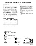
Page 42: ... identified by the mark in the schematic diagram and the parts list Before replacing any of these components read the parts list in this manual carefully The use of substitute replacement parts that do not have the same safety characteristics as speci fied in the parts list may create shock fire or other hazards Capacitor Temperature Markings Capacitors and transistors are represented by the fol l...

Page 43: ...umbers in the parts list section of the service manual 4 Wire Connectors 1 Prefix symbol CN means connector can disconnect and reconnect 2 Prefix symbol CL means wire solder holes of the PCB wire is soldered directly 5 Note Mark is a leadless chip component 6 Mode SP REC 7 Voltage indications for PLAY and REC modes on the schematics are as shown below 8 How to read converged lines 9 Test Point Inf...

Page 44: ...E2 E3 E4 F1 F2 F3 F4 Main 1 5 Schematic Diagram TV VCR Section 1 11 3 1 11 4 TD900SCM1 MAIN 1 5 Ref No Position IC1201 C 3 IC1202 D 1 Q1205 A 1 Q1206 D 3 Q1207 A 2 Q1210 A 2 Q1211 A 1 Q1212 D 3 CL1201 F 4 TP1201 B 4 ICS TRANSISTORS TEST POINT CONNECTOR ...

Page 45: ...IGNAL PB AUDIO TV VCR LINE SIGNAL 1 11 5 1 11 6 TD900SCM2 Main 2 5 Schematic Diagram TV VCR Section MAIN 2 5 Ref No Position IC1401 H 2 Q1401 K 2 Q1402 K 3 Q1403 K 4 Q1871 G 2 Q1872 H 1 Q1873 G 2 Q1874 G 1 Q1875 G 1 CL1401 G 3 CL1402 L 1 CL1403 L 1 TP1401 I 2 TP1402 K 3 TP1403 I 4 TP1802 G 2 IC TRANSISTORS CONNECTORS TEST POINTS ...

Page 46: ...C VIDEO SIGNAL PB VIDEO TV VCR LINE SIGNAL DVD VIDEO SIGNAL PB VIDEO TV VCR LINE DVD VIDEO SIGNAL 1 11 7 1 11 8 TD900SCM3 Main 3 5 Schematic Diagram TV VCR Section MAIN 3 5 Ref No Position IC1301 M 2 Q1010 Q 2 Q1301 M 1 Q1350 P 3 Q1351 O 4 CN1301 R 4 IC TRANSISTORS CONNECTOR ...

Page 47: ... V3 W1 W2 W3 S4 T4 U4 V4 W4 REC AUDIO SIGNAL PB AUDIO TV VCR LINE SIGNAL 1 11 9 1 11 10 TD900SCM4 Main 4 5 Schematic Diagram TV VCR Section MAIN 4 5 Ref No Position IC1751 T 2 Q1701 W 2 TP1701 T 2 TP1702 T 2 IC TRANSISTOR TEST POINTS ...

Page 48: ...V VCR LINE SIGNAL DVD AUDIO SIGNAL 1 11 11 1 11 12 TD900SCM5 Main 5 5 Schematic Diagram TV VCR Section MAIN 5 5 Ref No Position IC1602 Y 2 IC1801 AA 2 IC1802 X 4 Q1608 Z 2 Q1611 Y 2 Q1612 BB 3 Q1613 Y 1 Q1803 Y 3 Q1806 Y 4 CN1802 BB 1 CN1803 X 2 CN1804 CC 3 CN1805 CC 2 TP1632 Z 3 TP1801 Z 4 TEST POINTS ICS TRANSISTORS CONNECTORS ...

Page 49: ... the power supply circuit to fail Power Supply AV 1 2 Schematic Diagram TV VCR Section 1 11 13 1 11 14 TD900SCP1 VOLTAGE CHART Power off mode Ref No 1 4 IC2601 13 2 2 3 IC2602 2 0 IC2603 1 8 1 9 IC2604 0 Ref No Q2601 Ref No Q2602 Q2603 Q2604 Q2605 Q2606 Q2607 Q2608 Q2609 Q2610 Q2611 Q2612 Q2613 Q2614 Q2615 Q2617 S 0 E 0 0 6 8 0 10 3 0 0 1 5 9 10 3 0 2 0 0 9 0 9 0 0 2 2 12 1 0 0 3 0 D 140 7 C 1 4 4...

Page 50: ... Power Supply AV 2 2 Schematic Diagram TV VCR Section 1 11 15 1 11 16 TD900SCP2 POWER SUPPLY AV 2 2 Ref No Position IC2201 I 2 Q2202 I 4 Q2204 H 4 Q2205 J 4 Q2207 H 3 Q2210 I 3 Q2211 I 3 Q2614 H 3 Q2621 H 1 Q2622 H 1 Q2623 H 2 CN2401 L 3 CN2402 L 2 CN2803 G 4 TP2201 K 3 TP2202 K 3 TP2203 K 3 TP2204 K 3 TEST POINTS IC CONNECTORS TRANSISTORS ...

Page 51: ...2 E3 1 11 17 1 11 18 TD900SCHV H V Schematic Diagram TV VCR Section H V Ref No Position IC551 B 3 Q571 C 1 Q591 B 1 Q592 B 1 CL501A E 1 CL502A E 1 CL503A A 2 CN571 C 3 J520 D 1 J521 D 2 J522 C 1 J535 D 2 TEST POINTS IC TRANSISTORS CONNECTORS ...

Page 52: ... DVD AUDIO SIGNAL PB VIDEO TV VCR LINE DVD VIDEO SIGNAL 1 11 19 1 11 20 TD900SCCRT CRT Schematic Diagram TV VCR Section TD900SCF Function Schematic Diagram TV VCR Section CRT Ref No Position Q501 A 2 Q502 B 2 Q503 B 1 Q504 A 1 Q505 B 1 Q506 B 1 CL501 A 2 CL504A A 2 CN501A C 1 TRANSISTORS CONNECTORS ...

Page 53: ...EO AUDIO TRACKING SERVO SIGNAL SPINDLE SERVO SIGNAL SLED SERVO SIGNAL 1 11 21 1 11 22 TD900SCD1 DVD Main 1 3 Schematic Diagram DVD Section DVD MAIN 1 3 Ref No Position IC201 B 1 IC202 E 4 IC301 D 3 IC461 E 1 Q251 C 2 Q252 B 2 Q253 C 2 Q254 B 2 CN201 A 3 CN301 A 1 CN401 F 3 CONNECTORS ICS TRANSISTORS ...

Page 54: ... K4 L1 L2 L3 L4 DVD VIDEO SIGNAL DATA VIDEO AUDIO SPINDLE SERVO SIGNAL SLED SERVO SIGNAL FOCUS SERVO SIGNAL TRACKING SERVO SIGNAL DATA AUDIO SIGNAL 1 11 23 1 11 24 TD900SCD2 DVD Main 2 3 Schematic Diagram DVD Section DVD MAIN 2 3 Ref No Position IC101 H 4 IC ...

Page 55: ...4 0 1 127 2 0 2 0 32 64 96 3 4 3 4 128 2 0 2 0 PIN NO PLAY STOP PIN NO PLAY STOP PIN NO PLAY STOP PIN NO PLAY STOP 129 2 0 2 0 161 193 225 1 9 1 9 130 2 2 2 2 162 1 4 1 4 194 0 0 226 3 3 3 3 131 2 3 2 3 163 195 3 3 3 3 227 132 0 4 0 1 164 0 9 0 9 196 228 133 1 2 0 4 165 3 3 3 3 197 229 134 0 4 0 1 166 1 5 1 5 198 0 0 230 0 0 135 0 2 0 2 167 0 0 199 231 136 2 3 2 3 168 2 1 2 1 200 232 3 3 3 3 137 1...

Page 56: ...2 Q3 Q4 R1 R2 R3 R4 DVD AUDIO SIGNAL DVD VIDEO SIGNAL DATA AUDIO SIGNAL 1 11 27 1 11 28 TD900SCD3 DVD Main 3 3 Schematic Diagram DVD Section DVD MAIN 3 3 Ref No Position IC102 O 4 IC103 O 3 IC104 N 3 IC105 N 1 IC451 P 3 IC601 Q 1 CN601 R 1 ICS CONNECTOR ...

Page 57: ...1602 A 1 IC1751 C 2 IC1801 A 3 IC1802 B 2 Q1010 A 5 Q1205 F 2 Q1206 E 3 Q1207 F 2 Q1210 F 1 Q1211 F 1 Q1212 E 1 Q1301 A 4 Q1350 B 5 Q1351 A 4 Q1401 E 3 Q1402 D 3 Q1403 D 2 Q1608 A 2 Q1611 A 1 Q1612 E 2 Q1613 B 1 Q1701 C 3 Q1803 B 2 Q1806 B 3 Q1871 C 3 Q1872 C 3 Q1873 C 3 Q1874 C 3 Q1875 C 3 CL1201 D 5 CL1401 D 2 CL1402 D 4 CL1403 D 1 CN1301 C 5 CN1802 E 5 CN1803 A 1 CN1804 B 1 CN1805 F 1 TP1201 B ...

Page 58: ...PIN 58 OF IC1201 PIN 59 OF IC1201 PIN 61 OF IC1401 PIN 42 OF IC1401 PIN 7 OF IC1401 WF8 WF4 WF16 WF15 WF2 PIN 41 OF IC1301 WF9 Main CBA Bottom View TV VCR Section 1 11 31 1 11 32 BTD850F01012 ...

Page 59: ...ÊME TYPE DE 4A 125V 4A 125V CAUTION Fixed voltage or Auto voltage selectable power supply circuit is used in this unit If Main Fuse F2601 is blown check to see that all components in the power supply circuit are not defective before you connect the AC plug to the AC power supply Otherwise it may cause some components in the power supply circuit to fail POWER SUPPLY AV CBA Ref No Position IC2201 D ...

Page 60: ... parts in hot circuit is measured using hot GND as a common terminal CAUTION FOR CONTINUED PROTECTION AGAINST RISK OF FIRE REPLACE ONLY WITH SAME TYPE 4A 125V FUSE ATTENTION UTILISER UN FUSIBLE DE RECHANGE DE MÊME TYPE DE 4A 125V 4A 125V CAUTION Fixed voltage or Auto voltage selectable power supply circuit is used in this unit If Main Fuse F2601 is blown check to see that all components in the pow...

Page 61: ... GND J535 X RAY CHK J520 J522 H V CBA Top View TV VCR Section 1 11 37 1 11 38 BTD930F01031 A H V CBA Ref No Position IC551 B 1 Q571 B 1 Q591 B 1 Q592 C 2 CL501A B 2 CL502A C 1 CL503A C 1 CN571 A 1 J520 B 2 J521 B 2 J522 B 2 J535 B 2 TEST POINTS TRANSISTORS IC CONNECTORS ...

Page 62: ...WF11 PIN 5 OF CN571 Q571 Collector WF10 H V CBA Bottom View TV VCR Section 1 11 39 1 11 40 BTD930F01031 A ...

Page 63: ... Q501 Collector 1 11 41 1 11 42 CRT CBA Top View TV VCR Section CRT CBA Bottom View TV VCR Section BTD930F01031 B CRT CBA Ref No Position Q501 A 1 Q502 B 2 Q503 B 2 Q504 A 1 Q505 B 1 Q506 B 2 CL501 A 2 CL504A B 1 CN501 A 1 TRANSISTORS CONNECTORS ...

Page 64: ...1 11 43 BTD850F01022B 1 11 44 Function CBA Top View TV VCR Section Function CBA Bottom View TV VCR Section ...

Page 65: ...ction A CBA Top View TV VCR Section Junction A CBA Bottom View TV VCR Section Junction B CBA Top View TV VCR Section Junction B CBA Bottom View TV VCR Section 1 11 45 1 11 46 BTD930F01031 D BTD930F01031 C ...

Page 66: ... V 10 ms 0 5 ms 1 V 20 µs 20 µs 200 V 10 V 5 ms 20 V 20 µs 20 V 20 µs WF15MAIN 1 5 SCHEMATIC DIAGRAM IC1201 PIN 58 1 V WF16MAIN 1 5 SCHEMATIC DIAGRAM IC1201 PIN 59 1 V 5 ms 20 µs WF12CRT SCHEMATIC DIAGRAM Q501 COLLECTOR 20 V 20 µs WF18 POWER SUPPLY AV 2 2 SCHEMATIC DIAGRAM TP2203 DVD Y POWER SUPPLY AV 2 2 SCHEMATIC DIAGRAM TP2204 DVD C POWER SUPPLY AV 2 2 SCHEMATIC DIAGRAM CN2401 PIN 6 POWER SUPPL...

Page 67: ...4 A B SENSOR CBA ST SENSOR BHB300F01014 A B Hi Fi A L 1 Hi Fi COM 2 Hi Fi A R 3 V R 2 4 V COM 5 V L 2 6 V L 1 7 V COM 8 V R 1 9 AE H 1 AE H FE H 2 A COM 3 A PB REC 4 CTL 5 CTL 6 FE H 1 FE H GND 2 P SAFETY2 1 GND 1 BLUE 2 GREEN 3 RED 4 SPOT KILL 5 P SAFETY1 2 FBP 3 H DRIVE 4 V RAMP FB 5 GND 6 ACL ABL 7 V DRIVE 8 GND 9 BLUE 10 GREEN 11 RED 12 SPOT KILL 13 P SAFETY2 1 P SAFETY1 2 FBP 3 H DRIVE 4 V RA...

Page 68: ...ND 2 E 3 DVD ON 5V 4 VREF 5 B 6 C 7 D 8 A 9 CD DVD 10 F 11 GND LD 12 CD LD 13 PD MONI 14 DVD LD 15 GND DVD PD 16 GND CD PD 17 TS 18 FS 19 FS 20 TS TO CN2402 TO CN2401 SPDIF 12 AUDIO 5V 11 NU 10 DVD AUDIO R 9 NU 8 DVD AUDIO L 7 DVD A MUTE 6 GND 5 GND 4 DVD C 3 GND 2 DVD Y 1 EV 1 5V 1 EV 1 5V 2 EV 1 5V 3 EV 3 3V 4 EV 3 3V 5 GND 6 GND 7 GND 8 GND 9 GND 10 GND 11 GND 12 DVD ON 5V 13 AL 9V 14 AL 9V 15 ...

Page 69: ...V SF 1 51V 1 98V 1 80V SM 3 20V 3 75V 3 40V AU 0 26V 0 65V 0 44V AL 4 51V 5 00V 5 00V SS 2 61V 3 19V 2 97V RS Note Note EJ RS Loading FWD LM FWD REV H RS EJ Loading REV LM FWD REV L Stop A Loading Stop B Unloading Note Symbol Loading Status EJ Eject CL Eject REW Reel SB REW Reel Stop B TL Stop B Brake Cancel FB Brake Cancel FF REW SF FF REW Stop M FF REW SM Stop M FF REW Stop A AU Stop A Play REC ...

Page 70: ...TL 66 C F R STILL STILL FRAME ADVANCE ROLL COMPENSATION DRUM SERVO H A SW 15 ROTA AT The first rise of RF SW after a rise in F AD signal ST T1 BL H H T2 Z 1 SP MODE 1 2 3 4 Acceleration Detection Stop Detection Slow Tracking Value Reversal Limit Value Chart 1 ...

Page 71: ... 66 C F R STILL STILL FRAME ADVANCE ROLL COMPENSATION DRUM SERVO H A SW 15 ROTA AT The first rise of RF SW after a rise in F AD signal ST T1 BL H H T2 Z 2 LP EP MODE 1 2 3 4 Acceleration Detection Stop Detection Slow Tracking Value Reversal Limit Value Chart 2 ...

Page 72: ...V LD REV LD FWD LD REV LD REV LD REV 0 2S 0 5S CL EJ SS SS AU AU TL Z ON ON PAUSE SLOW AU AL AL AU SF SM POWER OFF STOP PLAY RS FS STILL SLOW PLAY STOP PLAY SB TL SB FB SM SM SF AL AL RS AU AL SS AU AL SM 0 8S 0 2S 0 3S 1 0S 0 2S 0 5S 0 12S 0 8S 0 2S 1 2S 0 2S 20mS 0 4S 40mS 0 2S 0 2S Refer to STILL SLOW TIMING CHART 1 2 0 3S 0 2S 20mS 40mS 0 4S 0 2S 0 2S 0 2S 0 3S REC SFT SW POWER STOP B PIN NO L...

Page 73: ...REV FF LD REV LD REV LD FWD LD FWD LD FWD LD FWD LD FWD LD FWD LD FWD REC PAUSE REC REC REW LD REV LD REV LD REV LD REV LD REV LD REV LD REV PAUSE REC or PAUSE STOP EJECT STOP EJECT STOP EJECT 2 STOP A FF STOP A REW STOP A REC PAUSE PAUSE or REC STOP A EJECT STOP FF STOP REW STOP REC REC REC PAUSE STOP TL TL SM SM SF SF AL AL SM AL AL AL AU AU SM TL SB EJ RS RS SM SM SF FB SM AU AU SS SS SS SF AU ...

Page 74: ...ray Open Tray IN TL221 3 3V 0V 0V 3 3V 0V 1 65V 0V 0V 0V 1 65V 1 65V 1 65V Tray OUT TL220 Sled Drive TP303 Disc Drive TP301 Focus Drive TP304 Tracking Drive Tracking Drive TP302 Tray Close Disc Rotation Play Disc Stop Tray Open DVD SECTION ...

Page 75: ...ntrol Signal 24 NU Not Used 25 DVD REMOTE Remote Control Signal to DVD 26 OUT TV VCR LED TV VCR Mode LED Control Signal 27 OUT REC EE PB YCA IC Mode Output 28 IN OUT SP LP SLP Tape Speed Control Output 29 OUT EXT H External Input or Playback SIgnal Output 30 OUT RENTAL Rental Position Control Signal 31 OUT P ON H Power On Signal at High 32 OUT SPL PLAY Special Playback Control Signal 33 IN REC SAF...

Page 76: ...ONT Capstan Motor Control Signal 77 OUT D CONT Drum Motor Control Signal 78 IN P SAFETY 3 Power Supply Failure Detection 3 79 NU Not Used 80 IN T REEL Take Up Reel Rotation Signal 81 NU Not Used 82 OUT LD CONT Loading Motor Control Signal 83 NU Not Used 84 IN P DOWN Power Voltage Down Detector Signal 85 NU Not Used 86 NU Not Used 87 IN C FG Capstan Motor Rotation Detection Pulse 88 GND GND AMP 89 ...

Page 77: ...091M 80 51 81 100 1 30 50 31 5 4 8 1 BR24C02F W AT24C02N 10SC M24C02 MN6 BR24C02F CAT24WC02JI M24C02 WMN6 MID 32A22F E C 60 LA72670M A MPB E 21 40 41 20 1 80 61 R A K KIA431 AT 1 4 8 5 NJM4558D KIA4558P 1 2 3 4 PQ070XF01SZ PQ018EF01SZ 16 9 8 TC4053BF N CD4053BCSJX CD4053BNSR 1 42 22 21 M61276FP 1 Note A Anode K Cathode E Emitter C Collector B Base R Reference S Source G Gate D Drain 1 12 AN17805A ...

Page 78: ...ixtures and Tools 2 2 1 Mechanical Alignment Procedures 2 3 1 Disassembly Assembly Procedures of Deck Mechanism 2 4 1 Alignment Procedures of Mechanism 2 4 9 Sec 2 Deck Mechanism Section I Standard Maintenance I Alignment for Mechanism I Disassembly Assembly of Mechanism I Alignment Procedures of Mechanism ...

Page 79: ... only H Hours Check I Change Deck Periodic Service Schedule Ref No Part Name 1 000 H 2 000 H 3 000 H 4 000 H B2 Cylinder Assembly I I B3 Loading Motor Assembly I B8 Pulley Assembly I I B587 Tension Lever Assembly I I B31 AC Head Assembly I B573 B574 Reel SP D2 Reel TU D2 I B37 Capstan Motor I I B52 Cap Belt I I B73 FE Head I B133 B134 Idler Gear Idler Arm I I B410 Pinch Arm A Assembly I I B414 M B...

Page 80: ... hard material but since it is very thin avoid cleaning it vertically 2 Wait for the cleaned part to dry thoroughly before operating the unit 3 Do not reuse a stained head cleaning stick or a stained chamois cloth Cleaning of Audio Control Head Clean the head with a cotton swab Procedure 1 Remove the top cabinet 2 Dip the cotton swab in 90 isopropyl alcohol and clean the audio control head Be care...

Page 81: ...2 Alignment Tape FL8N 2Head only FL8NW 4Head only Azimuth and X Value Adjustment of Audio Control Head Adjustment of Envelope Waveform J 2 Guide Roller Adj Screwdriver Available Locally Guide Roller J 3 Mirror Available Locally Tape Transportation Check J 4 Azimuth Adj Screwdriver Available Locally A C Head Height J 5 X Value Adj Screwdriver Available Locally X Value ...

Page 82: ... that the Moving guide preparations are in the Eject Position 4 Turn the LDG Belt in the appropriate direction shown in Fig M1 until the Moving guide prepara tions come to the Eject Position Stop turning when the preparations begin clicking or can not be moved further However the tape will be left wound around the cylinder 5 Turn the LDG Belt in the appropriate direction con tinuously and the cass...

Page 83: ... the X value and envelope Not good Do the final tape traveling test to see that the tape runs normally in play mode with out creasing or slacking Completion Not good OK OK OK Not good Not good OK Flowchart of Alignment for tape traveling 1 A 1 A 1 B 1 C 1 C 1 D 1 D 1 B 1 C 1 B 1 C 1 A 1 Tape Interchangeability Alignment Note To do these alignment procedures make sure that the Tracking Control Circ...

Page 84: ... the Audio Control Erase Head Symptom of Misalignment If the Horizontal Position of the Audio Control Erase Head is not properly aligned maximum envelope can not be obtained at the Neutral position of the Tracking Control Circuit 1 Connect the oscilloscope to TP1403 HA MONI TOR and TP1201 CTL on the Main CBA Use TP1401 RF SW as a trigger 2 Playback the Gray Scale of the Alignment Tape FL8NW and co...

Page 85: ...own in Fig M7 adjust the height of Guide Roller 2 Refer to Fig M3 so that the waveform looks like the one shown in Fig M9 4 If the envelope is as shown in Fig M8 adjust the height of Guide Roller 3 Refer to Fig M3 so that the waveform looks like the one shown in Fig M9 5 When Guide Rollers 2 and 3 Refer to Fig M3 are aligned properly there is no envelope drop either at the beginning or end of trac...

Page 86: ... T DM1 DM6 Desolder 3 S 2 8 8 Loading Motor Assembly T DM1 DM7 Desolder LDG Belt 2 S 3 9 9 AC Head Assembly T DM1 DM7 S 4 10 2 Tape Guide Arm Assembly T DM1 DM8 P 2 11 10 C Door Opener T DM1 DM8 L 4 12 11 Pinch Arm B T DM1 DM8 P 3 13 12 Pinch Arm Assembly T DM1 DM8 14 14 FE Head Assembly T DM1 DM9 S 5 15 15 Prism T DM1 DM9 S 6 16 2 15 Sensor Gear T DM1 DM15 17 2 Slider Shaft T DM10 L 5 18 17 C Dri...

Page 87: ...r Installation Refer to Deck Exploded Views for lubrication 33 32 Loading Arm TU Assembly B DM2 DM14 Refer to Alignment Sec Pg 2 4 9 34 2 25 M Brake TU Assembly T DM1 DM15 P 7 Brake Belt 35 2 25 M Brake SP Assembly T DM1 DM15 P 8 36 35 Tension Lever Assembly T DM1 DM15 37 36 T Lever Holder T DM15 L 12 38 34 Reel TU D2 T DM1 DM15 39 38 M Gear T DM1 DM15 40 36 Reel SP D2 T DM1 DM15 41 32 36 Moving G...

Page 88: ...2 4 3 TD951DA 14 13 11 10 12 7 46 8 30 40 16 39 38 42 41 43 9 34 15 36 35 Fig DM1 Top View 29 32 20 33 24 25 27 26 23 28 31 21 22 Fig DM2 Bottom View ...

Page 89: ...ull up the right side on 2 to release Pin A and Pin B from the slots A Then remove Pin C and Pin D on 2 from the slots B as shown Fig DM4 2 Pin A Slots B Pin C Pin B Pin D Pull up Slide Slot A Slot A 1 2 A 3 4 5 6 L 1 L 2 P 1 Fig DM5 L 3 S 1A Fig DM6 View for A Desolder from bottom Lead with Red Stripe L 14 46 47 7 S 2 A ...

Page 90: ...Stripe A 8 9 S 4 S 3 LDG Belt 28 11 13 12 A 10 L 4 Adj Screw P 3 P 2 When reassembling 10 and 12 confirm that pin of 10 and pin of 12 are in the groove of 28 as shown Pin of 12 Pin of 10 Groove of 28 View for A Fig DM8 Fig DM9 14 15 S 6 S 5 16 Fig DM10 18 17 19 S 7 L 5 P 4 ...

Page 91: ...8 as shown in the left figure and then install 23 while pressing the spring P 5 to the direction of the arrow in the left figure and confirming that the position of the spring P 5 is placed as shown in the left figure Pin on 22 Position of pin on 22 Top View L 6 22 23 P 5 Pin on bottom of 23 23 21 C 1 C 4 ...

Page 92: ... 44 First groove on 28 Align 25 and 28 as shown Bottom View 28 Pin of 34 Pin of 31 Position of Mode Lever when installed Pin of 35 Fig DM13 25 24 C 3 S 9 25 27 26 28 C 2 L 8 L 9 L 10 Refer to the Alignment Section Page 2 4 9 Fig DM14 31 30 29 L 11 P 6 32 33 Fig DM15 35 37 turn turn 38 39 40 36 P 8 P 7 turn Break belt 34 L 12 ...

Page 93: ...2 4 8 TD951DA Fig DM16 41 42 43 L 13 44 45 P 9 Slide Fig DM17 ...

Page 94: ... the mechanical or electrical parts Alignment points in Eject Position Alignment 1 Loading Arm SP and TU Assembly Install Loading Arm SP and TU Assembly so that their triangle marks point to each other as shown in Fig AL2 Alignment 2 Mode Gear Keeping the two triangles pointing at each other install the Loading Arm SP Assembly so that the last tooth of the gear meets the most inside teeth of the M...

Page 95: ...D TABLE OF CONTENTS Cabinet Exploded Views 3 1 1 Packing Exploded Views 3 1 3 Deck Mechanism Exploded Views 3 1 4 Mechanical Parts List 3 2 1 Electrical Parts List 3 3 1 Deck Parts List 3 4 1 Sec 3 Exploded views and Parts List Section I Exploded views I Parts List ...

Page 96: ...DL2 DL1 DL1 DB1 A1 9 A1X TB24 TL1 TL1 TL1 1B2 1B1 CL2402 CL2401 B6 SP1802 CL1802 L4 B6 L4 SP2801 CL2801 CLN551 V501 L551 B4 A4 DG601 TB14 TL5 See Electrical Parts List for parts with this mark Power Supply AV CBA Sensor CBA Sensor CBA Junction A CBA Main CBA H V CBA Function CBA Junction B CBA DVD Main CBA Unit CRT CBA B7 TB19 TL1 W2601 Details for L551 and surrounding parts SHINWHA TAPE SGT 730 W...

Page 97: ...3 1 3 TD900PEX S4 S1 X1 TAPE X5 X4 X2 X3 S3 S6 S7 S2 PACKING TAPE Packing ...

Page 98: ...Chassis Assembly Bottom View Lubricating Point B2 B35 B410 B411 B494 B567 L1053 B74 B10 L1191 B73 B9 B12 B492 B11 B571 B37 B126 L1466 B501 B8 B121 B426 B560 L1450 L1450 L1051 L1467 B553 Mark Description Floil G 684G or Multemp MH D Blue grease SLIDUS OIL 150 DECK EXPLODED VIEWS Deck Mechanism View 1 ...

Page 99: ...se point B516 B559 A B52 B507 B488 B134 B133 B568 B593 B570 B491 B565 L1151 B525 B592 B31 L1406 B148 B521 B520 B590 B564 B487 B573 B574 B499 B587 B508 B558 B557 B3 B417 B591 B522 B414 B416 Mark Description Floil G 684G or Multemp MH D Blue grease SLIDUS OIL 150 SANKOUL FG84M Yellow grease B513 B502 Deck Mechanism View 2 ...

Page 100: ...B563 B300 B562 B482 B355 B354 B483 B425 L1321 B347 L1321 B361 B359 B529 B360 B514 B313 Some Ref Numbers are not in sequence Mark Description Floil G 684G or Multemp MH D Blue grease SLIDUS OIL 150 B561 L1341 Deck Mechanism View 3 ...

Page 101: ...01 DEGAUSSING COIL AVDG187 or LLBH00ZWR053 DEGAUSSING COIL F 053 LLBH00ZTM053 L1 SCREW P TIGHT 4X18 BIND HEAD GBMP4180 L2 SCREW TAPPING M4X14 DBU14140 L3 SCREW P TIGHT 3X10 BIND HEAD GBKP3100 L4 SCREW P TIGHT 3X10 BIND HEAD GBMP3100 SP1802 SPEAKER S0407F01A DSD0807XQ001 SP2801 SPEAKER S0407F01A DSD0807XQ001 TB1 TRAY CHASSIS TD851UB 0EM000766 TB2 TOP SHIELD T5400UA 0EM201663 TB6 SHIELD BOX X4 TD801...

Page 102: ...OLYTIC CAP 47µF 6 3V M H7 CE0KMAVSL470 C1221 CERAMIC CAP AX B K 0 01µF 50V CCA1JKT0B103 C1222 CERAMIC CAP AX X M 2200pF 16V CCA1CMT0X222 C1223 ELECTROLYTIC CAP 1µF 50V M H7 CE1JMAVSL1R0 C1224 CERAMIC CAP AX B K 1000pF 50V CCA1JKT0B102 C1225 CERAMIC CAP AX B K 560pF 50V CCA1JKT0B561 C1226 CERAMIC CAP AX B K 1000pF 50V CCA1JKT0B102 C1233 CERAMIC CAP AX B K 0 01µF 50V CCA1JKT0B103 C1235 CERAMIC CAP A...

Page 103: ...1J473TU011 C1444 ELECTROLYTIC CAP 22µF 16V M H7 CE1CMAVSL220 C1445 CERAMIC CAP AX B K 0 01µF 50V CCA1JKT0B103 Ref No Description Part No C1446 ELECTROLYTIC CAP 1µF 50V M or CE1JMASDL1R0 ELECTROLYTIC CAP 1µF 50V M or CE1JMASDL010 ELECTROLYTIC CAP 1µF 50V M CE1JMASTL1R0 C1447 CERAMIC CAP AX B K 0 01µF 50V CCA1JKT0B103 C1449 CERAMIC CAP AX F Z 0 1µF 50V CCA1JZTFZ104 C1452 CERAMIC CAP AX F Z 0 022µF 2...

Page 104: ...µF 6 3V M CE0KMASTL101 C1800 CERAMIC CAP AX F Z 0 1µF 50V CCA1JZTFZ104 C1802 ELECTROLYTIC CAP 22µF 50V M or CE1JMASDL220 Ref No Description Part No ELECTROLYTIC CAP 22µF 50V M CE1JMASTL220 C1803 PCB JUMPER D0 6 P5 0 JW5 0T C1804 ELECTROLYTIC CAP 100µF 16V M or CE1CMASDL101 ELECTROLYTIC CAP 100µF 16V M CE1CMASTL101 C1805 ELECTROLYTIC CAP 1µF 50V M or CE1JMASDL1R0 ELECTROLYTIC CAP 1µF 50V M or CE1JM...

Page 105: ...QDTZ001SS133 SWITCHING DIODE 1N4148 NDTZ001N4148 D1350 SWITCHING DIODE 1SS133 T 77 or QDTZ001SS133 SWITCHING DIODE 1N4148 NDTZ001N4148 Ref No Description Part No D1351 SWITCHING DIODE 1SS133 T 77 or QDTZ001SS133 SWITCHING DIODE 1N4148 NDTZ001N4148 D1352 ZENER DIODE MTZJT 779 1B or QDTB0MTZJ9R1 ZENER DIODE DZ 9 1BSBT265 NDTB0DZ9R1BS D1353 ZENER DIODE MTZJT 779 1B or QDTB0MTZJ9R1 ZENER DIODE DZ 9 1B...

Page 106: ...on Part No TRANSISTOR 2SC2785 J or QQSJ02SC2785 TRANSISTOR KTC3199 GR or NQS10KTC3199 TRANSISTOR KTC3198 GR or NQS40KTC3198 TRANSISTOR 2SC1815 GR TPE2 QQS102SC1815 Q1401 TRANSISTOR 2SA1175 F or QQSF02SA1175 TRANSISTOR KTA1267 GR or NQS10KTA1267 TRANSISTOR KTA1266 GR or NQS40KTA1266 TRANSISTOR 2SA1015 GR TPE2 QQS102SA1015 Q1402 TRANSISTOR 2SA1175 F or QQSF02SA1175 TRANSISTOR KTA1267 GR or NQS10KTA1...

Page 107: ...CX4JATZ0562 R1260 PCB JUMPER D0 6 P5 0 JW5 0T R1262 CARBON RES 1 4W J 4 7k Ω RCX4JATZ0472 Ref No Description Part No R1263 CARBON RES 1 4W J 39k Ω RCX4JATZ0393 R1267 CARBON RES 1 4W J 33k Ω RCX4JATZ0333 R1269 PCB JUMPER D0 6 P5 0 JW5 0T R1270 CARBON RES 1 4W J 100k Ω RCX4JATZ0104 R1271 CARBON RES 1 4W J 10k Ω RCX4JATZ0103 R1272 CARBON RES 1 4W J 10k Ω RCX4JATZ0103 R1273 CARBON RES 1 4W J 1 8k Ω RC...

Page 108: ... RES 1 4W J 47k Ω RCX4JATZ0473 R1824 CARBON RES 1 4W J 47k Ω RCX4JATZ0473 R1825 CARBON RES 1 4W J 47k Ω RCX4JATZ0473 R1826 CARBON RES 1 4W J 47k Ω RCX4JATZ0473 Ref No Description Part No R1827 CARBON RES 1 4W J 47k Ω RCX4JATZ0473 R1828 CARBON RES 1 4W J 47k Ω RCX4JATZ0473 R1829 CARBON RES 1 4W J 47k Ω RCX4JATZ0473 R1853 CARBON RES 1 4W J 2 2M Ω RCX4JATZ0225 R1856 CARBON RES 1 4W J 12k Ω RCX4JATZ01...

Page 109: ...545MHz 20PPM or FXC355LJNY01 X TAL 3 579545MHz 20PPM or FXC355LLN003 X TAL 3 579545MHz 20PPM or FXC355LDS001 X TAL 3 579545MHz or FXC355LLN001 X TAL 3 579545MHz 20PPM FXC355LCHE01 Ref No Description Part No Ref No Description Part No SENSOR CBA Consists of the following 0ESA04524 TRANSISTORS Q201 PHOTO TRANSISTOR MID 32A22F NPWZ1D32A22F Q202 PHOTO TRANSISTOR MID 32A22F NPWZ1D32A22F Ref No Descript...

Page 110: ...4 METAL OXIDE FILM RES 2W J 100 Ω or RN02101DP004 METAL OXIDE FILM RES 2W J 100 Ω RN02101ZU001 Ref No Description Part No R550 CARBON RES 1 4W J 2 2k Ω RCX4JATZ0222 R551 CARBON RES 1 4W J 1 5k Ω RCX4JATZ0152 R552 CARBON RES 1 4W J 2 2k Ω RCX4JATZ0222 R555 PCB JUMPER D0 6 P5 0 JW5 0T R556 CARBON RES 1 4W J 1 Ω RCX4JATZ0010 R557 CARBON RES 1 4W J 470 Ω RCX4JATZ0471 R558 CARBON RES 1 4W J 47k Ω RCX4J...

Page 111: ...5 F or QQSF02SC2785 TRANSISTOR 2SC2785 H or QQSH02SC2785 TRANSISTOR 2SC2785 J or QQSJ02SC2785 TRANSISTOR KTC3199 GR or NQS10KTC3199 TRANSISTOR KTC3198 GR or NQS40KTC3198 TRANSISTOR 2SC1815 GR TPE2 QQS102SC1815 RESISTORS R501 CARBON RES 1 4W J 100 Ω RCX4JATZ0101 R502 CARBON RES 1 4W J 100 Ω RCX4JATZ0101 R503 CARBON RES 1 4W J 100 Ω RCX4JATZ0101 R504 PCB JUMPER D0 6 P5 0 JW5 0T R505 PCB JUMPER D0 6 ...

Page 112: ... 082µF 50V J or CMA1JJS00823 FILM CAP P 0 082µF 50V J CA1J823MS029 C2615 CERAMIC CAP BN 820pF 2KV or CCD3DKA0B821 Ref No Description Part No CERAMIC CAP 820pF 2KV or CA3D821PAN04 CERAMIC CAP RB 820pF 2KV CA3D821TE006 C2616 ELECTROLYTIC CAP 100µF 160V M or CE2CMZPDL101 ELECTROLYTIC CAP 100µF 160V M or CE2CMZPTL101 ELECTROLYTIC CAP 100µF 160V M W F CE2CMZNTL101 C2617 ELECTROLYTIC CAP 470µF 35V M or ...

Page 113: ...148 NDTZ001N4148 D2640 DIODE 1ZC33 or QDQZ0001ZC33 ZENER DIODE RD33FB QDQZ000RD33F D2641 ZENER DIODE MTZJT 7736A or QDTA00MTZJ36 ZENER DIODE DZ 36BSAT265 NDTA00DZ36BS Ref No Description Part No D2644 ZENER DIODE MTZJT 775 6C or QDTC0MTZJ5R6 ZENER DIODE DZ 5 6BSCT265 NDTC0DZ5R6BS D2645 SCHOTTKY BARRIER DIODE 21DQ04 or QDQZ0021DQ04 SCHOTTKY BARRIER DIODE ERB81 004 AERB81004 D2646 SCHOTTKY BARRIER DI...

Page 114: ...QQS102SC1815 Q2612 TRANSISTOR 2SC2785 F or QQSF02SC2785 Ref No Description Part No TRANSISTOR 2SC2785 H or QQSH02SC2785 TRANSISTOR 2SC2785 J or QQSJ02SC2785 TRANSISTOR KTC3199 GR or NQS10KTC3199 TRANSISTOR KTC3198 GR or NQS40KTC3198 TRANSISTOR 2SC1815 GR TPE2 QQS102SC1815 Q2613 TRANSISTOR 2SC2120 O TPE2 or QQS002SC2120 TRANSISTOR 2SC2120 Y TPE2 QQSY02SC2120 Q2614 TRANSISTOR 2SC2120 O TPE2 or QQS00...

Page 115: ...ZU001 METAL OXIDE FILM RES 1W J 8 2 Ω RN018R2DP003 R2651 CARBON RES 1 4W J 47k Ω RCX4JATZ0473 Ref No Description Part No R2653 CARBON RES 1 4W J 270 Ω RCX4JATZ0271 R2654 CARBON RES 1 2W J 15 Ω or RCX2JZQZ0150 CARBON RES 1 2W J 15 Ω RCX2150KA013 R2655 CARBON RES 1 4W J 2 7k Ω RCX4JATZ0272 R2656 CARBON RES 1 4W J 22k Ω RCX4JATZ0223 R2657 CARBON RES 1 4W J 22k Ω RCX4JATZ0223 R2659 CARBON RES 1 4W J 2...

Page 116: ...TZ0152 R2402 CARBON RES 1 4W G 1 5k Ω RCX4GATZ0152 R2403 CARBON RES 1 4W G 2 2k Ω RCX4GATZ0222 R2404 CARBON RES 1 4W G 2 7k Ω RCX4GATZ0272 R2405 CARBON RES 1 4W G 4 7k Ω RCX4GATZ0472 R2406 CARBON RES 1 4W G 6 8k Ω RCX4GATZ0682 R2407 CARBON RES 1 4W G 15k Ω RCX4GATZ0153 SWITCHES SW2401 TACT SWITCH SKQSAB or SST0101AL038 TACT SWITCH SKHHAM or SST0101AL029 TACT SWITCH KSM0612B or SST0101HH003 TACT SW...

Page 117: ...R MK9 0VM410032C B361 CL POST MK10 0VM411114 B410 PINCH ARM A ASSEMBLY 4 MK12 or 0VSA13572 PINCH ARM A ASSEMBLY 5 MK12 0VSA13788 B411 PINCH SPRING MK12 0VM414644 B414 M BRAKE SP ASSEMBLY MK12 0VSA13282 B416 M BRAKE TU ASSEMBLY MK12 0VSA13283 B417 TENSION SPG 3002645 MK12 0VM414221F B425 LOCK LEVER SPRING MK10 0VM411110 B426 KICK PULLEY MK10 0VM411095 B482 CASSETTE PLATE MK12 0VM203749 B483 LOCK LE...

Page 118: ...1321 SCREW S TIGHT M3X6 BIND HEAD GBMS3060 L1341 SCREW P TIGHT M2X6 PAN HEAD GPMP2060 L1406 AC HEAD SCREW MK9 0VM410964 L1450 SCREW SEMS M2 6X5 PAN HEAD CPM39050 L1466 SCREW S TIGHT M2 6X6 BIND HEAD GBMS9060 L1467 SCREW M2 6X5 WASHER HEAD SCM39050 Ref No Description Part No ...

Page 119: ...Printed in Japan 2003 08 25 HO 6720FDD TD900UA ...

Reviews: