4.10
61
4.10.3 Power Board_PCB2 Bias Supply Circuit (0558038315)
SECTION 4
DESCRIPTION Of OPERATION
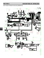
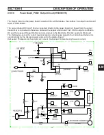
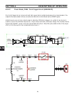
The Bias supply circuit provides the power necessary to operate the onboard circuitry of the PC1600. This
section provides three output voltages to the unit; +15VDC, -15VDC and +5 VDC.
Two 18 VAC inputs are applied to the board at J20 Pins 4, 5 and 6, With pin 5 being the grounded center
tap off the transformer.
This AC power is applied to a full wave rectifier,
BR1 where it is converted to a pulsing 25 VDC. This puls-
ing DC is then filtered and passed to the regulator circuits.
The positive 15 VDC supply is filtered by C71 and C72, a pair of 1000 mfd capacitors. This power is then
connected to a five pin adjustable voltage regulator, U13. Output voltage is set by the voltage divider com
-
prised of R94, R95 and R96. Pin 4 of the voltage regulator is connected to R95 a 500 trim pot that is used
to adjust the output voltage of the regulator. Output power is turned on or off by turning on the mosfet Q4.
When Q4 is forward biased, the Mosfet conducts and places a low on pin 5 of the regulator U13. The Q4
MOSFET is turned on by the microcontroller on the Power Board PCB2.
Power output from the regulator is filtered by C73 and C76, a pair of 1000 mfd capacitors, before being
passed to the needed circuitry.
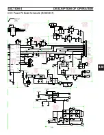
The Negative output of the rectifier bridge
BR1 is connected to Q5, which acts as a series pass device.
When Q5 is turned on, it allows power to be passed to the negative voltage regulator. Q5 is turned on when
Q6 is conducting. Q6 is placed in conduction when the microcontroller passes the enable_n15 signal to
the base of Q6. In this manner, the microcontroller on the Power Board can control the power supply. Once
Q5 is turned on and passing current, the negative supply is filtered by C77, a 1000 mfd filter capacitor. This
filtered output is then fed to U15 a three pin -15VDC regulator.
The +5vdc supply is fed from the positive filter section (C71 and C72) and connected to a three pin adjust
-
able regulator U14. The output of this regulator is varied by R112 a 500 Ohm trim pot. This supply is always
active whenever the machine is powered up.
Summary of Contents for PowerCut 1600
Page 16: ...3 0 16 section 3 SPECIFICATIONS 3 4 Machine Operation Flowchart...
Page 27: ...4 2 27 4 2 Control Transformer T2 0558007188 SECTION 4 DESCRIPTION OF OPERATION...
Page 30: ...4 3 30 4 3 Input Bridge 0558007068 0558007077 SECTION 4 DESCRIPTION OF OPERATION...
Page 35: ...4 6 35 blank...
Page 38: ...4 8 38 4 8 PCB1 Control Board 0558038317 SECTION 4 DESCRIPTION OF OPERATION 4 10 6 8 5 3 11 7...
Page 52: ...4 8 52 4 8 14 PCB1 Layout 0558038317 SECTION 4 DESCRIPTION OF OPERATION...
Page 60: ...4 10 60 4 10 2 Power PC Board Schematic 2 0558038315 SECTION 4 DESCRIPTION OF OPERATION 3 14 8...
Page 67: ...4 10 67 4 10 7 Power Board_PCB2 Control Relays 0558038315 SECTION 4 DESCRIPTION OF OPERATION...
Page 77: ...4 10 77 4 10 16 Buss Supply IGBT SECTION 4 DESCRIPTION OF OPERATION...
Page 91: ...4 11 91 4 11 Power Driver 0558038335 SECTION 4 DESCRIPTION OF OPERATION...
Page 109: ...4 19 109 SECTION 4 DESCRIPTION OF OPERATION 4 19 PT38 Plasma Torch...
Page 110: ...4 19 110 SECTION 4 DESCRIPTION OF OPERATION 4 19 PT38 Plasma Torch...
Page 113: ...5 0 113 5 1 Wiring Diagram 230 460 Volt 0558007543 section 5 WIring diagrams...
Page 114: ...5 0 114 5 1 Wiring Diagram 230 460 Volt 0558007543 section 5 WIring diagrams...
Page 115: ...5 0 115 5 1 Wiring Diagram 230 460 Volt 0558007543 section 5 WIring diagrams...
Page 116: ...5 0 116 section 5 WIring diagrams 5 1 Wiring Diagram 230 460 Volt 0558007543...
Page 117: ...5 0 117 section 5 WIring diagrams 5 1 Wiring Diagram 230 460 Volt 0558007543...
Page 118: ...5 0 118 5 2 Wiring Diagram 400 400V CE 0558007547 section 5 WIring diagrams...
Page 119: ...5 0 119 section 5 WIring diagrams 5 2 Wiring Diagram 400 400V CE 0558007547...
Page 120: ...5 0 120 5 2 Wiring Diagram 400 400V CE 0558007547 section 5 WIring diagrams...
Page 121: ...5 0 121 section 5 WIring diagrams 5 2 Wiring Diagram 400 400V CE 0558007547...
Page 122: ...5 0 122 5 2 Wiring Diagram 400 400V CE 0558007547 section 5 WIring diagrams...
Page 123: ...5 0 123 section 5 WIring diagrams 5 2 Wiring Diagram 400 400V CE 0558007547...
Page 124: ...124 5 3 Wiring Diagram 575V 0558007545 section 5 WIring diagrams...
Page 125: ...125 section 5 WIring diagrams 5 3 Wiring Diagram 575V 0558007545...
Page 126: ...126 5 3 Wiring Diagram 575V 0558007545 section 5 WIring diagrams...
Page 127: ...127 section 5 WIring diagrams 5 3 Wiring Diagram 575V 0558007545...
Page 128: ...128 5 3 Wiring Diagram 575V 0558007545 section 5 WIring diagrams...
Page 129: ...129 section 5 WIring diagrams 5 3 Wiring Diagram 575V 0558007545...
Page 130: ...130 blank...
Page 135: ...6 0 blank 135...
Page 136: ...6 0 136 section 6 replacement parts 6 3 Front 0558007540...
Page 140: ...6 0 140 6 3 Top 0558007540 section 6 replacement parts...
Page 144: ...6 0 144 section 6 replacement parts 6 3 Left Inside2 0558007540...
Page 146: ...6 0 146 section 6 replacement parts 6 3 Rear View 0558007540...
Page 148: ...6 0 148 6 3 Front Rear Isometric Views 0558007540 section 6 replacement parts...
Page 159: ...159 section 7 mechanized conversion 20 Trim all tie wraps and replace the unit s cover...
Page 166: ...10 166 SECTION 9 General information 10 3 Ohm s and Watt s Laws...
Page 171: ...10 171 10 6 Ohm Testing SECTION 9 General information...
Page 172: ...10 172 10 7 Diode Testing SECTION 9 General information...
Page 173: ...10 173 10 8 Ripple SECTION 9 General information...
Page 174: ...10 174 10 9 Voltage Measurement SECTION 9 General information...
Page 178: ...10 178 IGBT Tester Schematic 10 10 1 IGBT Testing SECTION 8 General information...
Page 182: ...182 revision history Original release 11 2008 1...

