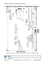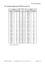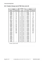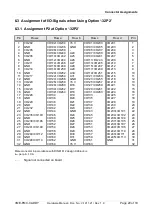
PCB View, Coding Switches, Configuration Resistors
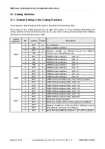
Coding
switches
Bit
Setting
Value
Description
S200
8
OFF
0
least decoded VMEbus address = A30 of PCI-address
7
OFF
0
least decoded VMEbus address = A29 of PCI-address
6
OFF
0
least decoded VMEbus address = A28 of PCI-address
5
OFF
0
most decoded VMEbus address = A31 of PCI-address
4
OFF
0
most decoded VMEbus address = A30 of PCI-address
3
OFF
0
most decoded VMEbus address = A29 of PCI-address
2
OFF
0
most decoded VMEbus address = A28 of PCI-address
1
OFF
0
Universe register in PCI-I/O-space
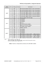
S213
8
OFF
0
no evaluation
7
OFF
0
no evaluation
6
OFF
0
no evaluation
5
OFF
0
PKG-size
4
OFF
0
DY4-auto-ID-mode: disabled
3
OFF
0
VME64-auto-ID-mode: disabled
2
OFF
0
bus-isolation mode: enabled
1
ON
1
SYSFAIL: disabled
S300 *
8
OFF
0
no evaluation
7
OFF
0
no evaluation
6
OFF
0
no evaluation
5
OFF
0
no evaluation
4
OFF
0
IRQ-mapping on PCI-bus (INTD1 ↔ INTA2): disabled
3
OFF
0
IRQ-mapping on PCI-bus (INTC1 ↔ INTD2): disabled
2
OFF
0
IRQ-mapping on PCI-bus (INTB1 ↔ INTC2): disabled
1
OFF
0
IRQ-mapping on PCI-bus (INTA1 ↔ INTB2): disabled
* Note:
S300 is equipped for special cases only.
S300 is not equipped on the VME-PMC-CADDY versions with the following order numbers:
V.1911.01, V.1911.02, V.1911.10 and V.1911.11.
Table 4:
Position of coding switches at delivery of the VME-PMC-CADDY
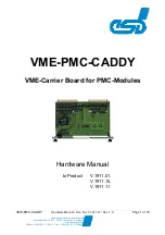
VME-PMC-CADDY
Hardware Manual • Doc. No.: V.1911.21 / Rev. 1.9
Page 15 of 33

