background image

Hardware Installation

5. Hardware Installation

NOTICE

Read the safety instructions at the beginning of this document carefully, before 
you start with the hardware installation!

DANGER

Hazardous Voltage - 

Risk of electric shock

 due to unintentional contact with 

uninsulated live parts with high voltages inside of the system into which the VME-PMC-
CADDY is to be integrated.  
→ Disconnect all hazardous voltages (mains voltage) before opening the system. 
→ Ensure the absence of voltage before starting any electrical work 

NOTICE

Electrostatic discharges may cause damage to electronic components. 


To avoid this, please discharge the static electricity from your body by touching the
metal case of the


VMEbus system 

before

 you touch the VME-PMC-CADDY.

Furthermore, you should prevent your clothes from touching the VME-PMC-CADDY,
because your clothes might be electrostatically charged as well.

Procedure:

1.

Switch off your system and all connected peripheral devices (monitor, printer, etc.).

2.

Discharge your body as described above.

3.

Disconnect the system from the mains. 

DANGER

Hazardous Voltage

Risk of electric shock

 due to unintentional contact with uninsulated live parts with 

high voltages. 


Disconnect all hazardous voltages (mains voltage) before opening the system. 
If the system does not have a flexible mains cable, but is directly connected to 
mains, disconnect the power supply via the safety fuse and make sure that the fuse
cannot switch on again unintentionally (i.e. with caution label).
Ensure the absence of voltage before starting any electrical work. 

4.

Open the case if necessary.

5.

Install the PMC boards on the VME-PMC-CADDY carrier board.

6.

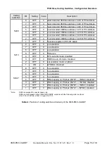
If necessary, configure the coding switches as described in chapter “Coding Switches” on 
page 14. 

7.

Insert the VME-PMC-CADDY board into the selected VME


slot. Carefully push the board until

it snaps into place.

8.

Close the system's case again.

9.

Connect the system to mains again (mains connector or safety fuse).

10. Switch on the system and the peripheral devices. - End of hardware installation.

VME-PMC-CADDY

Hardware Manual • Doc. No.: V.1911.21 / Rev. 1.9

Page 23 of 33

Summary of Contents for VME-PMC-CADDY

Page 1: ...Manual to Product V 1911 01 V 1911 10 V 1911 11 VME PMC CADDY Hardware Manual Doc No V 1911 21 Rev 1 9 Page 1 of 33 esd electronic system design gmbh Vahrenwalder Str 207 30165 Hannover Germany http www esd eu Phone 49 0 511 3 72 98 0 Fax 49 0 511 3 72 98 68 ...

Page 2: ...c system design gmbh Hannover esd electronic system design gmbh Vahrenwalder Str 207 30165 Hannover Germany Phone 49 511 372 98 0 Fax 49 511 372 98 68 E Mail info esd eu Internet www esd eu This manual contains important information and instructions on safe and efficient handling of the VME PMC CADDY Carefully read this manual before commencing any work and follow the instructions The manual is a ...

Page 3: ...rmation and Classification of Warning messages inserted Manual restructured 2016 10 24 1 1 Description revised 1 2 1 Extended temperature range option deleted 1 2 2 New Chapter VMEbus 1 2 3 Standard corrected 2 Notes inserted 2 2 1 Notice inserted 3 Manufacturer of PCI bridge component changed link updated 4 Chaptee Front Panel with LEDs moved 5 New Chapter Hardware Installation 6 Chapter Connecto...

Page 4: ...ements indicate a hazardous situation which if not avoided will result in death or serious injury WARNING Warning statements indicate a hazardous situation that if not avoided could result in death or serious injury CAUTION Caution statements indicate a hazardous situation that if not avoided could result in minor or moderate injury NOTICE Notice statements are used to notify people on hazards tha...

Page 5: ...nsure an ambient temperature as specified in the technical data DANGER Hazardous Voltage Risk of electric shock due to unintentional contact with uninsulated live parts with high voltages inside of the system into which the VME PMC CADDY is to be integrated Disconnect all hazardous voltages mains voltage before opening the system Ensure the absence of voltage before starting any electrical work NO...

Page 6: ...ADDY does not require any manual configuration of the hardware Unauthorized intervention in the device voids warranty claims Disposal Devices which have become defective in the long run have to be disposed in an appropriate way or have to be returned to the manufacturer for proper disposal Please make a contribution to environmental protection Number Representation All numbers in this document are...

Page 7: ...y Voltage via VMEbus RX620 RX625 20 3 Address Assignment of the VME PMC CADDY 21 4 Front Panel with LEDs 22 5 Hardware Installation 23 6 Connector Assignments 24 6 1 VMEbus P1 24 6 2 Standard Assignment of I O Signals 25 6 2 1 Standard Assignment P2 25 6 2 2 Standard Assignment of an Interface Module with Signals of Rows a and c from P2 26 6 2 3 Standard Assignment of PMC Connector J14 27 6 2 4 St...

Page 8: ... according to the draft standard IEEE P1386 Draft 2 0 except the standard I O pin routing It is possible therefore to insert all PMC modules which are on the market that can handle 5 V signalling on PCI bus In addition to the connectors for the PMC address data and control signals every plug in unit of the VME PMC CADDY has an I O connector which applies the I O signals of the PMC modules to VMEbu...

Page 9: ...terrupt lines of the PMC module in slot 1 with the interrupt lines of the PMC module in slot 2 The front panel of the VME PMC CADDY has two cut outs for the front panels of the PMC modules A blank cover for unused positions is part of the product package VME PMC CADDY Hardware Manual Doc No V 1911 21 Rev 1 9 Page 9 of 33 ...

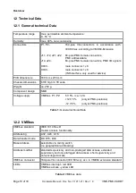
Page 10: ...Component design SMD Voltage supply VMEbus P1 P2 5 V 5 ca 1 2 A 12 V 5 only at PMC positions 12 V 5 only at PMC positions Table 1 General technical Data 1 2 2 VMEbus VMEbus standard IEEE 1014 Rev D master or slave functionality Addressing A32 A24 A16 Data transfer mode D8 D16 D32 Base address selectable via coding switch no geographical addressing Address modifier standard supervisory and non priv...

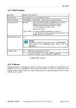
Page 11: ...d and z Signal Voltage Level 5V NOTICE 3 3V PMC modules are only usable if they are 5V tolerant PMC modules with 3 3V only signal voltage level are forbidden Voltage supply 5 V VMEbus voltage supply via P1 P2 3 3 V via voltage control from 5 V of the VMEbus each max 1 5 A load current or via option 3 3P1 directly from VME64 P1 Table 3 PMC positions 1 2 4 Software Example libraries for initializing...

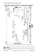
Page 12: ...nfiguration Resistors Figure 2 Position of connectors and configuration resistors on the VME PMC CADDY NOTICE Read chapter Hardware Installation on page 23 before you start with the installation of the hardware Page 12 of 33 Hardware Manual Doc No V 1911 21 Rev 1 9 VME PMC CADDY ...

Page 13: ...n Resistors Figure 3 Position of coding switches and configuration resistors on the bottom layer of the PCB See also from page 24 for signal assignment of the connectors VME PMC CADDY Hardware Manual Doc No V 1911 21 Rev 1 9 Page 13 of 33 ...

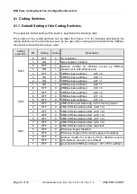
Page 14: ... 1 VMEbus base address A22 1 2 ON 1 VMEbus base address A21 1 1 ON 1 VMEbus base address A20 1 S202 8 OFF 0 VMEbus base address A19 0 7 OFF 0 VMEbus base address A18 0 6 OFF 0 VMEbus base address A17 0 5 OFF 0 VMEbus base address A16 0 4 OFF 0 VME control and status reg in PCI memory space 3 OFF 0 VME CSR translation offset A20 0 2 OFF 0 VME CSR translation offset A19 0 1 OFF 0 VME CSR translation...

Page 15: ... 6 OFF 0 no evaluation 5 OFF 0 PKG size 4 OFF 0 DY4 auto ID mode disabled 3 OFF 0 VME64 auto ID mode disabled 2 OFF 0 bus isolation mode enabled 1 ON 1 SYSFAIL disabled S300 8 OFF 0 no evaluation 7 OFF 0 no evaluation 6 OFF 0 no evaluation 5 OFF 0 no evaluation 4 OFF 0 IRQ mapping on PCI bus INTD1 INTA2 disabled 3 OFF 0 IRQ mapping on PCI bus INTC1 INTD2 disabled 2 OFF 0 IRQ mapping on PCI bus INT...

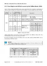
Page 16: ... address default A24 mode A31 A23 A15 3 ON 1 A30 A22 A14 2 ON 1 A29 A21 A13 1 ON 1 A28 A20 A12 Table 5 Coding switch S203 Coding switch S203 is just used to set the most significant four VMEbus address bits The following address bits are set by coding switch S202 By means of switches 5 and 6 the address area is set under which the PMC CADDY can be accessed by the VMEbus master NOTICE If the select...

Page 17: ...bus base address default A24 mode A27 A19 don t care 7 OFF 1 A26 A18 don t care 6 OFF 1 A25 A17 don t care 5 OFF 1 A24 A16 don t care 4 OFF 0 VME control and status reg in PCI memory space 3 OFF 0 VME CSR translation offset A20 0 2 OFF 0 VME CSR translation offset A19 0 1 OFF 0 VME CSR translation offset A18 0 Table 7 Coding switch S202 VME PMC CADDY Hardware Manual Doc No V 1911 21 Rev 1 9 Page 1...

Page 18: ...1 and 2 are routed to the VMEbus If the coding switch contacts are closed the interrupt lines of the modules are additionally connected from one PMC module to the other Coding switch Bit Switch Value IRQ Mapping S300 4 OFF 0 INTD1 INTA2 disabled 3 OFF 0 INTC1 INTD2 disabled 2 OFF 0 INTB1 INTC2 disabled 1 OFF 0 INTA1 INTB2 disabled Figure 4 Connecting P1 and P2 via jumper S300 Page 18 of 33 Hardwar...

Page 19: ...ignals on Rows a and c of P2 By means of option 32P2 the assignment of rows a and c of the P2 connector changes as specified in table 6 3 in the Standard IEEE P1386 Draft 2 0 The pins of PMC connector J14 are still connected to those of the P2 connector as described above All 64 I O signals are fed to rows a and c of the P2 connector Parallel to this pins 33 64 of PMC connector J24 are also fed to...

Page 20: ...3V supply voltage is fed for both PMC modules by the ten according pins of VME64 connector P1 For option 3 3P1 the six resistors RX620 to RX625 have to be equipped The resistors are in 0805 design and have a value of 0 Ω Furthermore the following components have to be removed Voltage regulators U600 and U610 inductors L600 and L610 and the resistors R600 and R610 NOTICE Changing the component equi...

Page 21: ...endix of the manual of the PCI bridge component Appendix A Register the registers are specified which can be accessed via the base address specified above with according offset The complete UNIVERSE CA91C142D manual in PDF format can be downloaded from the IDT website http www idt com There the updated error lists to the manual of the component can be found too VME PMC CADDY Hardware Manual Doc No...

Page 22: ... 22 of 33 Hardware Manual Doc No V 1911 21 Rev 1 9 VME PMC CADDY IRQ BUSY PMC CADDY P M C S L O T 2 P M C S L O T 1 Interrupt LED red LED is on if an interrupt is triggered on the VMEbus Busy LED yellow LED is on if the board is accessed by the VMEbus ...

Page 23: ...devices monitor printer etc 2 Discharge your body as described above 3 Disconnect the system from the mains DANGER Hazardous Voltage Risk of electric shock due to unintentional contact with uninsulated live parts with high voltages Disconnect all hazardous voltages mains voltage before opening the system If the system does not have a flexible mains cable but is directly connected to mains disconne...

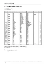
Page 24: ...5 V BBSY BCLR ACFAIL BG0IN BG0OUT BG1IN BG1OUT BG2IN BG2OUT BG3IN BG3OUT BR0 BR1 BR2 BR3 AM0 AM1 AM2 AM3 GND GND IRQ7 IRQ6 IRQ5 IRQ4 IRQ3 IRQ2 IRQ1 5 V D08 D09 D10 D11 D12 D13 D14 D15 GND SYSFAIL BERR SYSRESET LWORD AM5 A23 A22 A21 A20 A19 A18 A17 A16 A15 A14 A13 A12 A11 A10 A09 A08 12 V 5 V GND GND 1 2 3 4 5 6 7 8 9 10 11 12 13 14 15 16 17 18 19 20 21 22 23 24 25 26 27 28 29 30 31 32 Male connect...

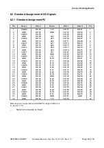
Page 25: ...ND A24 A25 A26 A27 A28 A29 A30 A31 GND 5 V D16 D17 D18 D19 D20 D21 D22 D23 GND D24 D25 D26 D27 D28 D29 D30 D31 GND 5 V I O101 I O103 I O105 I O107 I O109 I O111 I O113 I O115 I O117 I O119 I O121 I O123 I O125 I O127 I O129 I O131 I O133 I O135 I O137 I O139 I O141 I O143 I O145 I O147 I O149 I O151 I O153 I O155 I O157 I O159 I O161 I O163 I O201 I O203 I O204 I O206 I O207 I O209 I O210 I O212 I...

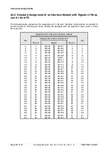
Page 26: ...17 18 19 20 21 22 23 24 25 26 27 28 29 30 31 32 I O102 I O104 I O106 I O108 I O110 I O112 I O114 I O116 I O118 I O120 I O122 I O124 I O126 I O128 I O130 I O132 I O134 I O136 I O138 I O140 I O142 I O144 I O146 I O148 I O150 I O152 I O154 I O156 I O158 I O160 I O162 I O164 I O101 I O103 I O105 I O107 I O109 I O111 I O113 I O115 I O117 I O119 I O121 I O123 I O125 I O127 I O129 I O131 I O133 I O135 I ...

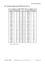
Page 27: ...c26 c27 c28 c29 c30 c31 c32 1 3 5 7 9 11 13 15 17 19 21 23 25 27 29 31 33 35 37 39 41 43 45 47 49 51 53 55 57 59 61 63 2 4 6 8 10 12 14 16 18 20 22 24 26 28 30 32 34 36 38 40 42 44 46 48 50 52 54 56 58 60 62 64 I O102 I O104 I O106 I O108 I O110 I O112 I O114 I O116 I O118 I O120 I O122 I O124 I O126 I O128 I O130 I O132 I O134 I O136 I O138 I O140 I O142 I O144 I O146 I O148 I O150 I O152 I O154 ...

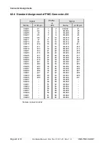
Page 28: ...d22 z23 d25 d26 z27 d29 d30 1 3 5 7 9 11 13 15 17 19 21 23 25 27 29 31 33 35 37 39 41 43 45 47 49 51 53 55 57 59 61 63 2 4 6 8 10 12 14 16 18 20 22 24 26 28 30 32 34 36 38 40 42 44 46 48 50 52 54 56 58 60 62 64 I O202 I O204 I O206 I O208 I O210 I O212 I O214 I O216 I O218 I O220 I O222 I O224 I O226 I O228 I O230 I O232 I O234 I O236 I O238 I O240 I O242 I O244 I O246 I O248 I O250 I O252 I O254 ...

Page 29: ...24 A25 A26 A27 A28 A29 A30 A31 GND 5 V D16 D17 D18 D19 D20 D21 D22 D23 GND D24 D25 D26 D27 D28 D29 D30 D31 GND 5 V I O101 I O233 I O103 I O235 I O105 I O237 I O107 I O239 I O109 I O241 I O111 I O243 I O113 I O245 I O115 I O247 I O117 I O249 I O119 I O251 I O121 I O253 I O123 I O255 I O125 I O257 I O127 I O259 I O129 I O261 I O131 I O263 I O133 I O135 I O137 I O139 I O141 I O143 I O145 I O147 I O14...

Page 30: ...O244 I O114 I O246 I O116 I O248 I O118 I O250 I O120 I O252 I O122 I O254 I O124 I O256 I O126 I O258 I O128 I O260 I O130 I O262 I O132 I O264 I O134 I O136 I O138 I O140 I O142 I O144 I O146 I O148 I O150 I O152 I O154 I O156 I O158 I O160 I O162 I O164 I O101 I O233 I O103 I O235 I O105 I O237 I O107 I O239 I O109 I O241 I O111 I O243 I O113 I O245 I O115 I O247 I O117 I O249 I O119 I O251 I O...

Page 31: ...8 10 12 14 16 18 20 22 24 26 28 30 32 34 36 38 40 42 44 46 48 50 52 54 56 58 60 62 64 34 36 38 40 42 44 46 48 50 52 54 56 58 60 62 64 a1 a2 a3 a4 a5 a6 a7 a8 a9 a10 a11 a12 a13 a14 a15 a16 a17 a18 a19 a20 a21 a22 a23 a24 a25 a26 a27 a28 a29 a30 a31 a32 d23 d24 z25 d27 d28 z29 z31 I O102 I O104 I O106 I O108 I O110 I O112 I O114 I O116 I O118 I O120 I O122 I O124 I O126 I O128 I O130 I O132 I O134 ...

Page 32: ...1 13 15 17 19 21 23 25 27 29 31 1 3 5 7 9 11 13 15 17 19 21 23 25 27 29 31 33 35 37 39 41 43 45 47 49 51 53 55 57 59 61 63 2 4 6 8 10 12 14 16 18 20 22 24 26 28 30 32 34 36 38 40 42 44 46 48 50 52 54 56 58 60 62 64 2 4 6 8 10 12 14 16 18 20 22 24 26 28 30 32 z1 d3 d4 z5 d7 d8 z9 d11 d12 z13 d15 d16 z17 d19 d20 z21 d23 d24 z25 d27 d28 z29 z31 a1 a2 a3 a4 a5 a6 a7 a8 a9 a10 a11 a12 a13 a14 a15 a16 I...

Page 33: ...OS 9 LIB Library for OS 9 to support access to PCI Devices as C Source V 1911 56 For detailed information about the driver availability for your special operating system please contact our sales team Table 8 Order information PDF Manuals Manuals are available in English and usually in German as well For availability of English manuals see table below Please download the manuals as PDF documents fr...

Reviews: