background image

   Configuration

   Hardware Manual • Doc. No.: V.1915.23/ Rev. 1.0 

VME-PMC-CADDY/2plus

Page 22 of  47

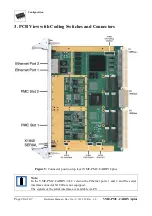
3.1 Default Setting of the Coding Switches

The default settings of the board as delivered is shown in the following table. 
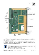
The coding switches are positioned on the bottom layer. The position of the coding switch can be taken
from figure 6. In the following description they are shown as if the board is viewed with the VMEbus
connectors on the right (view from PMC slot side).

Coding switch 

Setting Value

Description

SW600

8

OFF

1

SFAILEN Control Bit Reset Value

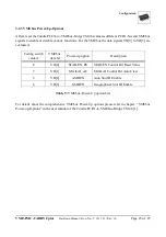
VMEbus Power Up Options

7

OFF

1

SFAILAI Control Bit Auto Clear

6

ON

0

Auto Slot ID Enable

5

ON

0

Geographical Slot ID Enable

4

OFF

1

not used

3

OFF

1

not used

2

OFF

1

VMEbus System Controller:
Default: System Controller Function disabled

1

ON

0

SW800

4

OFF

1

PMC module 1 is not configured as Monarch

3

OFF

1

PMC module 2 is not configured as Monarch

2

ON

0

PCI-Bus of the PMC module is set to the fixed value of 33 MHz

1

OFF

1

(PUPEN) reserved for future applications

SW100

4

OFF

0

VME Signal V-SERCLK is not connected to PMC Signal I/O204

3

OFF

0

VME Signal V-SERCLK is not connected to PMC-Signal I/O104

2

OFF

0

VME Signal V-SERDAT is not connected to PMC-Signal I/O204

1

OFF

0

VME Signal V-SERDAT is not connected to PMC-Signal I/O104

*) For details on the evaluation of the bits see [1].

Table 6: Overview of the default setting of the coding switches

Summary of Contents for V.1915.04

Page 1: ...ctronic system design gmbh Vahrenwalder Str 207 30165 Hannover Germany http www esd eu Phone 49 0 511 3 72 98 0 Fax 49 0 511 3 72 98 68 VME PMC CADDY 2plus VME Carrier Board for two PMC Modules VME PM...

Page 2: ...ny of its products to improve reliability performance or design All rights to this documentation are reserved by esd Distribution to third parties and reproduction of this document in any form whole o...

Page 3: ...us Rev 3 0 VME PMC CADDY 2 CC from serial number S N GL000318 Changes in the chapters The changes in the document listed below affect changes in the hardware and firmware as well as changes in the des...

Page 4: ...se discharge your personal static electricity before you touch the module Qualified Personal This documentation is directed exclusively towards qualified personal in control and automation engineering...

Page 5: ...3 2 3 VMEbus Power Up Options 25 3 3 PMC Slot Configuration SW800 26 3 4 Connect Special VME Signals to PMC I O Signals SW100 27 4 Hardware Installation 28 5 Address Assignment of VME PMC CADDY 2plus...

Page 6: ...Hardware Manual Doc No V 1915 23 Rev 1 0 VME PMC CADDY 2plus Page 6 of 47 9 Order Information 46...

Page 7: ...mes dev null or stdio h The following indicators are used to highlight noticeable descriptions Attention Warnings or cautions to tell you about operations which might have unwanted side effects Note N...

Page 8: ...us If the board operates as master it supports a 4 level arbiter The VMEbus interrupt can be applied to any of the seven interrupt request lines The VME PMC CADDY 2plus is connected to the VMEbus by t...

Page 9: ...is connected to exactly one pin of the VMEbus connector P2 according to VITA 35 P4V2 64ac and each of the I O pins of the PMC slot 2 J24 is connected with exactly one I O pin of the VMEbus connector P...

Page 10: ...Overview Hardware Manual Doc No V 1915 23 Rev 1 0 VME PMC CADDY 2plus Page 10 of 47 Figure 2 Conduction cooled version VME PMC CADDY 2 CC...

Page 11: ...nded temperature range 40 75 C order no V 1915 06 Conduction cooled 40 75 C order no V 1915 04 Humidity max 90 non condensing Connectors P1 P2 160 pin VG connector according to DIN 41612 in compliance...

Page 12: ...5 only to PMC slots VME PMC CADDY 2 CC VMEbus P1 P2 5 V 5 typical 2 A current consumption 3 3 V 5 ca 400mA Table 1 General technical data 1 4 2 Serial Interfaces Number 2 Control UART im MPC8349 Signa...

Page 13: ...2 CC version Number 2x Gigabit Ethernet VME PMC CADDY 2plus and VME PMC CADDY 2plus T only Standard IEEE802 3 10 BASE T 100BASE TX 1000BASE T Bit rate 10 Mbit s 100 Mbit s 1000 Mbit s Controller MPC83...

Page 14: ...e state of delivery the VME PMC CADDY 2plus and the VME PMC CADDY 2plus T are equipped with the SMD resistors RX2530 to RX2535 Thus the 3 3 V supply is generated onboard form the 5V power supply Optio...

Page 15: ...sumption 5 V max 1 0 A current consumption per PMC slot 12V max 1 0 A current consumption per PMC slot 12V max 1 0 A current consumption per PMC slot In the standard placement of the VME PMC CADDY 2 C...

Page 16: ...Panel and LEDs Hardware Manual Doc No V 1915 23 Rev 1 0 VME PMC CADDY 2plus Page 16 of 47 2 Front Panel and LEDs 2 1 VME PMC CADDY 2plus and VME PMC CADDY 2plus T Figure 3 Front of the VME PMC CADDY...

Page 17: ...LED Meaning LED on Labelling on front panel Name Colour Left LED of a socket Link 1000 green Link status Ethernet 1Gbit s connection to switch or hub resp available Right LED of a socket Link100 gree...

Page 18: ...8 of 47 2 2 VME PMC CADDY 2 CC Figure 4 Front of the conduction cooled version VME PMC CADDY 2 CC Note In the VME PMC CADDY 2 CC version the LEDs the Ethernet ports 1 and 2 and the serial interface co...

Page 19: ...of 47 2 3 Reset Button The reset button can be enabled by pushing with a non conducting bar shaped object max 1 5 mm diameter It triggers a local reset on the VME PMC CADDY 2plus or VME PMC CADDY 2 C...

Page 20: ...7 3 PCB View with Coding Switches and Connectors Figure 5 Connector position top layer VME PMC CADDY 2plus Note In the VME PMC CADDY 2 CC version the Ethernet ports 1 and 2 and the serial interface co...

Page 21: ...esistors RX130 RX135 are not equipped See chapter General technical Data on page 15 for information about the power supply voltages In the default version of the VME PMC CADDY 2 CC the SMD resistors R...

Page 22: ...it Auto Clear 6 ON 0 Auto Slot ID Enable 5 ON 0 Geographical Slot ID Enable 4 OFF 1 not used 3 OFF 1 not used 2 OFF 1 VMEbus System Controller Default System Controller Function disabled 1 ON 0 SW800...

Page 23: ...Overview Coding switch contact Bit name Function Default setting 8 SFAILEN Control Bit Reset Value VMEbus Power Up Options OFF 7 SFAILAI Control Bit Auto Clear OFF 6 Auto Slot ID Enable ON 5 Geograph...

Page 24: ...act 1 Function SCONEN SCONDIS OFF OFF Auto SCON automatic activation of the system controller depending of signal VBG3IN ON OFF System controller activated OFF ON System controller deactivated ON ON n...

Page 25: ...signals VD 0 to VD 3 are evaluated Coding switch contact VMEbus data bit Power up option Description 8 VD 0 SFAILEN_RV SFAILEN Control Bit Reset Value 7 VD 1 SFAILAI_AC SFAILAI Control Bit Auto Clear...

Page 26: ...2plus can be taken from figure 6 Coding switch contact Name Description Default 1 P PUPEN reserved for future applications always set to OFF OFF 2 P M66EN Clock rate of the PCI Bus of the PMC modules...

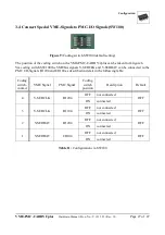
Page 27: ...switch SW100 the VMEbus signals V SERCLK and V SERDAT can be connected to the PMC I O Signals I O204 and I O104 as described in detail in the following table Coding switch contact VME Signal PMC Signa...

Page 28: ...us Voltage Risk of electric shock due to unintentional contact with uninsulated live parts with high voltages inside of the system into which theVME PMC CADDY 2plus is to be integrated Disconnect all...

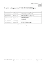
Page 29: ...PMC CADDY 2plus Address range Assignment 0x00000000 0x03ffffff DDR2 RAM 72 bit data width 0x80000000 0x8fffffff PCI Memory Space prefetchable 0x90000000 0x9fffffff PCI Memory Space 0xe0000000 0xe00ff...

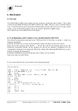
Page 30: ...nfiguration and Console Access Serial Interface RS 232 The default communication parameters are 9600 baud 8N1 8 data bits no parity 1 stopbit no hardware handshake After the next power on you will see...

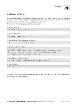
Page 31: ...nfiguration That means the bootloader environment variables ipaddr and serverip must be set up according to your network When any of the following steps fail do not proceed 1 Set the server IP 2 Set t...

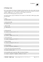
Page 32: ...er environment variables ipaddr netmask gatewayip and serverip must be set up according to your network When any of the following step fail do not proceed See chapter Booting VxWorks 1 Upload the new...

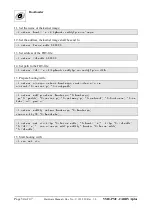
Page 33: ...be set up according to your network When any of the following steps fail do not proceed The first three steps areonlyfor VME PMC CPU 2 modules For VME PMC CADDY 2plus modules start with step 4 1 Load...

Page 34: ...LD MEJENHIIEMOPQQRSNLTCMOPQQRSNLTC QEH 15 Prepare booting with AB CDEDFG FJCPYWC CDEDFG HIIEPYWC YIIEAMQDGMFJC Y FJCYIIEA_ aCDYGDYKNbc_ aYIIENPEdb AB CDEDFG PQQKN CDEDFG HIIEPYWC _ aHIIEPYWCb KNA_ aKN...

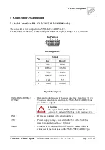
Page 35: ...CTSS1 c TXS2 RXS2 d RTSS2 CTSS2 e GND 5V z Shield Shield Signal description TXSx RXSx RTSSx CTSSx Data and control signals of the serial interfaces 1 and 2 x 1 2 The signal direction is seen from the...

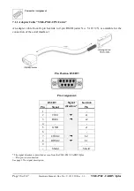
Page 36: ...r link to 9 pin DSUB order No V 1917 25 is available for the connection of the serial interface 1 Pin Position DSUB9 Pin Assignment DSUB9 Signal direction har link Pin Signal Pin 1 2 TXS1 a1 3 RXS1 a2...

Page 37: ...of the serial interfaces 1 and 2 Pin Position in the DSUB9 Socket Pin Assignment DSUB9 1 Signal direction har link DSUB9 2 Signal direction har link Pin Signal Pin Pin Signal Pin 1 1 2 TXS1 a1 2 TXS2...

Page 38: ...5 sockets 8P8C according to TIA 568A B Pin Position Cut out for fastening lever Pin Assignment Pin Signal 1 MDI0 TP0 2 MDI0 TP0 3 MDI1 TP1 4 MDI2 TP2 5 MDI2 TP2 6 MDI1 TP1 7 MDI3 TP3 8 MDI3 TP3 S Shie...

Page 39: ...4 A07 A06 A05 A04 A03 A02 A01 12 V 5 V BBSY BCLR ACFAIL BG0IN BG0OUT BG1IN BG1OUT BG2IN BG2OUT BG3IN BG3OUT BR0 BR1 BR2 BR3 AM0 AM1 AM2 AM3 GND GND IRQ7 IRQ6 IRQ5 IRQ4 IRQ3 IRQ2 IRQ1 5V STBY 5 V D08 D...

Page 40: ...I O114 I O116 I O118 I O120 I O122 I O124 I O126 I O128 I O130 I O132 I O134 I O136 I O138 I O140 I O142 I O144 I O146 I O148 I O150 I O152 I O154 I O156 I O158 I O160 I O162 I O164 5 V GND BRETRY A2...

Page 41: ...4 26 28 30 32 34 36 38 40 42 44 46 48 50 52 54 56 58 60 62 64 1 2 3 4 5 6 7 8 9 10 11 12 13 14 15 16 17 18 19 20 21 22 23 24 25 26 27 28 29 30 31 32 I O102 I O104 I O106 I O108 I O110 I O112 I O114 I...

Page 42: ...I O233 I O234 I O235 14 GND I O236 I O237 I O238 I O239 I O240 15 GND I O241 I O242 I O243 I O244 I O245 16 GND I O246 I O247 I O248 I O249 I O250 17 GND I O251 I O252 I O253 I O254 I O255 18 GND I O...

Page 43: ...c5 c6 c7 c8 c9 c10 c11 c12 c13 c14 c15 c16 c17 c18 c19 c20 c21 c22 c23 c24 c25 c26 c27 c28 c29 c30 c31 c32 1 3 5 7 9 11 13 15 17 19 21 23 25 27 29 31 33 35 37 39 41 43 45 47 49 51 53 55 57 59 61 63 2...

Page 44: ...d5 b5 e6 c6 a6 d7 b7 e8 c8 a8 d12 b12 e13 c13 a13 d14 b14 e15 c15 a15 d16 b16 e17 c17 a17 d18 b18 e19 c19 1 3 5 7 9 11 13 15 17 19 21 23 25 27 29 31 33 35 37 39 41 43 45 47 49 51 53 55 57 59 61 63 2...

Page 45: ...v 1 0 Page 45 of 47 8 References 1 Tsi148 PCI X to VME Bus Bridge User Manual Tundra Semiconductor Corporation referenced document version 80A3020_MA001_10 April 2008 The manual can be downloaded from...

Page 46: ...40 75 C Conduction Cooled V 1915 04 Accessories VME PMC CPU Cable Adapter cable for serial interface 1 RS 232 from har link10 to DSUB9 socket length 1 0 m For details see page 36 V 1917 25 VME PMC CPU...

Page 47: ...ge 47 of 47 Manuals Order No VME PMC CADDY 2plus ME Hardware manual in English V 1915 23 Table 14 Available manuals Printed Manuals If you need a printout of the manual additionally please contact our...

Reviews: