PB1650DAC1.1 D/A Piggyback (4 Channels)
22
2.3
Block Diagram
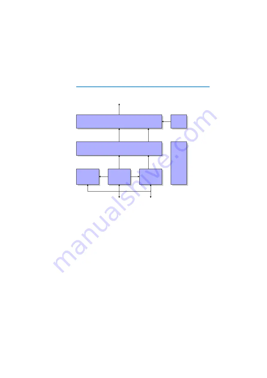
The block diagram below illustrates the working principle of the piggyback.
Fig. 2-1
PB1650DAC1.1 Block Diagram
At the bottom left of the block diagram, you see the control interface of the
piggyback that on the one hand is connected with the VMEbus and passes
data and the clock signal to the digital/analog converter through an
optocoupler. Signals are transferred between the VMEbus and the piggyback
via the 16-bit shift register at the bottom right of the diagram. The D/A
converter at the top of the diagram has eight output channels: four output
channels are used to generate the reference voltages for a channel and the
other four are used to generate the required analog voltage. The outputs can
be used in unipolar or bipolar mode.
D/A Converter
Optocoupler
Control
Logic
16 Bit Shift
Register
DC/DC
Conver-
ter
10 V
REF
ES1650.1
ID Byte
Analog Outputs 1-4
Data
Address and
Control Signals
Summary of Contents for ES1650.1
Page 1: ...ES1650 1 Piggyback Carrier Board User s Guide ...
Page 10: ...Introduction 10 ...
Page 20: ...20 Physical Dimensions Circuit board 100 x 160 mm Front panel Height 3 U Width 4 HP 20 3 mm ...
Page 45: ...45 Physical Dimensions Length 100 mm Width 48 mm Depth 12 mm ...
Page 46: ...46 ...
Page 64: ...PB1650PRT1 1 Prototyping Piggyback 64 ...
Page 82: ...82 ...


