25
The B16 jumper on the ES1650.1 carrier board has to be open for this address
range size.
2.5
Configuration
The PB1650DAC1.1 piggyback has four groups of solder straps on the solder
side, one group for each output channel. They are used to select the unipolar
or bipolar mode for the output voltage.
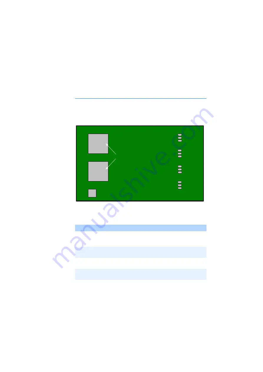
The position of each solder strap is shown in the following figure.
Fig. 2-4
Solder Side of the PB1650DAC1.1
The table provides you with an overview of the available functions and the
corresponding position of the solder straps.
Channel
Solder Strap Position
Function
A
BA2
1, 2 closed
1, 3 closed
Unipolar mode
Bipolar mode
(default setting: ds)
B
BB2
1, 2 closed
1, 3 closed
Unipolar mode
Bipolar mode (ds)
C
BC2
1, 2 closed
1, 3 closed
Unipolar mode
Bipolar mode (ds)
D
BD2
1, 2 closed
1, 3 closed
Unipolar mode
Bipolar mode (ds)
Tab. 2-1
Output voltage range of the PB1650DAC1.1
2
1
3
2
1
3
2
1
3
2
1
3
BD2
BC2
BB2
BA2
Calibration Unit
Serial Shift Register
Summary of Contents for ES1650.1
Page 1: ...ES1650 1 Piggyback Carrier Board User s Guide ...
Page 10: ...Introduction 10 ...
Page 20: ...20 Physical Dimensions Circuit board 100 x 160 mm Front panel Height 3 U Width 4 HP 20 3 mm ...
Page 45: ...45 Physical Dimensions Length 100 mm Width 48 mm Depth 12 mm ...
Page 46: ...46 ...
Page 64: ...PB1650PRT1 1 Prototyping Piggyback 64 ...
Page 82: ...82 ...


