51
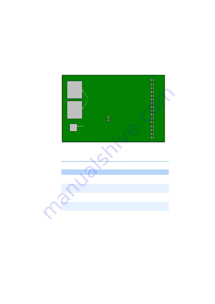
The figure below shows the position of the solder straps on the solder side of
the board.
Fig. 5-3
PB1650ADC1.1 Solder Side with Solder Straps
5.5.1
Input Voltage Range
The following table describes the function of each solder strap.
Input Channel
Solder Strap
Position
Input Voltage Range
0
BP0, BM0
Open
Closed
0-10 V and +/-10 V
0-5 V and +/-5 V
1
BP1, BM1
Open
Closed
0-10 V and +/-10 V
0-5 V and +/-5 V
2
BP2, BM2
Open
Closed
0-10 V and +/-10 V
0-5 V and +/-5 V
3
BP3, BM3
Open
Closed
0-10 V and +/-10 V
0-5 V and +/-5 V
4
BP4, BM4
Open
Closed
0-10 V and +/-10 V
0-5 V and +/-5 V
Tab. 5-1
Input Voltage Range of the PB1650ADC1.1
Serial Shift Register
Calibration Unit
BP7
BM7
BP6
BM6
BP5
BP4
BM4
BP3
BM3
BP2
BM2
BP1
BM1
BP0
BM0
B51
2
1
3
BM5
Summary of Contents for ES1650.1
Page 1: ...ES1650 1 Piggyback Carrier Board User s Guide ...
Page 10: ...Introduction 10 ...
Page 20: ...20 Physical Dimensions Circuit board 100 x 160 mm Front panel Height 3 U Width 4 HP 20 3 mm ...
Page 45: ...45 Physical Dimensions Length 100 mm Width 48 mm Depth 12 mm ...
Page 46: ...46 ...
Page 64: ...PB1650PRT1 1 Prototyping Piggyback 64 ...
Page 82: ...82 ...


