background image

Chapter 1  Introduction 

PISA-E1  User’s Manual 


Specifications  

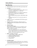
• 

Processor Socket

: Socket370 for FC-PGA and FC-PGA2 CPU. 

• 

Processor

:  


Intel FC-PGA/FC-PGA2 Pentium III 
600/650/667/750/800/850/866/933/1000/1113MHz/1.2G/1.4
G and above (100MHz FSB or 133 MHz FSB) 


Intel Celeron Processor 
533/566/600/633/337/700/733/766/800/850/900/1000/1200
MHz and above (66MHz FSB or 100MHz FSB) 


VIA C3 Processor 
700/766/800/866/933 MHz and above (66M/100M/133MHz 
FSB) 


Intel latest Tualatin and VIA C3 low power processors are 
supported. 

• 

Chipset

: VIA Twister-T and 82686B with PCI EIDE, Super-IO 

and RTC built-in. 

• 

Secondary Cache

: 512K(Tualatin), 256K(Coopermine) or 

128KB(Celeron) L2 cache integrated in CPU and runs on CPU 
core frequency. 

• 

Memory Sockets

:  

One 168-pin DIMM socket 
Memory types: 3.3V SDRAM (Synchronous DRAM) support 
8MB to 512MB memory capacity. Both ECC and non-ECC 
Memory module are supported. 

NOTE: Only SDRAM modules that support SPD (Serial 
Presence Detect) should be use. Use PC133 modules when 
running 133MHz Memory bus speed and use PC133/PC100 
modules when running133MHz memory bus speed. 

• 

BIOS

: Award BIOS, PnP support 


FLASH EEPROM (256KB) for BIOS update 


Enhanced ACPI BIOS and DMI 2.0 


ISA Plug and Play (PnP) extension 


Power management


Anti-Boot Virus


• 

DMI BIOS Support

       Desktop Management Interface (DMI) allows users to download 

system hardware-level information such as CPU type, CPU speed, 
internal/external frequencies and memory size. 

Summary of Contents for PISA-E1

Page 1: ...P PI IS SA A E E1 1 Pentium III Half Size CPU Card With VGA Audio Dual LAN User s Manual Version 1 4...

Page 2: ...r be liable for direct indirect special exemplary incidental incidental or consequential damages resulting from any defect or omission in this manual even if advised of possibility of such damages The...

Page 3: ...a 16 JP9 JP10 WatchDog Timer Period Selection 17 JPCOM4 COM2 RS232 RS422 RS485 Selection 17 Connectors on the PISA E1 18 Connector Locations on the PISA E1 19 Front Panel Connector 20 CPU Fan Power Co...

Page 4: ...ures 41 Integrated Peripherals 42 Power Management Setup 42 PnP PCI Configuration 42 PC Health Status 42 Frequency Voltage Control 42 Load Fail Safe Defaults 42 Load Optimized Defaults 42 Supervisor U...

Page 5: ...heable 53 Video RAM Cacheable 53 Frame Buffer Size 54 AGP Aperture Size 54 Panel Type 54 Boot Device Select 55 Power Supply Type 55 OnChip USB 55 USB Keyboard Support 55 USB Mouse Support 55 OnChip So...

Page 6: ...itoring 64 PnP PCI Configuration Setup 65 PNP OS Installed 65 Reset Configuration Data 65 Resource controlled by 65 IRQ Resources 66 DMA Resources 66 PCI VGA Palette Snoop 66 Assign IRQ For VGA USB 66...

Page 7: ...Contents PISA E1 User s Manual vii Appendix 72 A I O Port Address Map 73 B Interrupt Request Lines IRQ 74 C POST Beep 75...

Page 8: ......

Page 9: ...n PISA E1 User s Manual 1 1 Introduction This manual is designed to give you information on the PISA E1 SBC card The topics covered in this chapter are as follows Checklist Description Features Specif...

Page 10: ...6 chipset and is fully designed for harsh industrial environment It features one Socket370 that is compatible with Intel FC PGA package Pentium III processor This card accommodates up to 512MB of PC13...

Page 11: ...corporates the latest microprocessor technology to provide the increased bandwidth needed to operate your system bus at speeds up to 133 MHz The PISA E1 comes with VIA integrated hardware monitoring d...

Page 12: ...qual to CPU FSB and 33MHz or 33MHz of FSB Speed This gives users more flexibility to choose different memory technology ECC function support Processor front side bus FSB and Memory subsystem support E...

Page 13: ...tible serial ports and one parallel port with SPP EPP and ECP capabilities The COM4 can be configured as RS 232 RS 422 or RS485 interface IrDA Support an optional infrared port module for wireless int...

Page 14: ...alatin 256K Coopermine or 128KB Celeron L2 cache integrated in CPU and runs on CPU core frequency Memory Sockets One 168 pin DIMM socket Memory types 3 3V SDRAM Synchronous DRAM support 8MB to 512MB m...

Page 15: ...playback 2D 3D resolutions up to 1920x1440 Motion compensation for full speed DVD playback and MPEG 2 video textures Extensive LCD Support includes 36 bit DSTN TFT flat panel interface with 256 gray...

Page 16: ...ctable Green unction Power management via BIOS activated through mouse keyboard movement or SMI button Keyboard and Mouse Connectors One 6 pin mini DIN connector is located on the mounting bracket for...

Page 17: ...rve room for applications which require large frame buffer size Dual LAN Design Two 10 100M Ethernet provide aggregated bandwidth can be up to 400Mbps while two ports working on full duplex 100 BaseT...

Page 18: ...Chapter 1 Introduction 10 PISA E1 User s Manual This page is intentionally left blank...

Page 19: ...es information on how to use the jumpers and connectors on the PISA E1 in order to set up a workable system The topics covered are CPU Installation 12 Memory Installation 13 Jumpers on the PISA E1 13...

Page 20: ...he CPU with the correct orientation Use the notched corner of the CPU with the white dot as your guide The white dot should point towards the end of the lever Notice that there is a blank area where o...

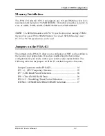
Page 21: ...ules meet PC133 or PC100 specification can be used Jumpers on the PISA E1 The jumpers on the PISA E1 allow you to configure your SBC card according to the needs of your applications If you have doubts...

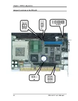
Page 22: ...Chapter 3 BIOS Configuration 14 PISA E1 User s Manual JP10 Jumper Locations on the PISA E1 JCOM4 JP5 JP6 JP8 JP9 P10 JP7...

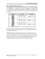
Page 23: ...6 Pin 2 3 Short 100MHz CPU FSB JP5 Pin 2 3 Short JP6 Pin 2 3 Short 66MHz CPU FSB The Core Frequency to Bus clock ratio of most of Intel Pentium III is locked Users do not require to change Jumpers JP4...

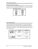
Page 24: ...AM Data This 3 pin Jumper allows the user to disconnect the built in 3V battery power to clear the information stored in the CMOS RAM To clear the CMOS data 1 Turn off the system power 2 Remove Jumper...

Page 25: ...e describes the jumper settings for the period JP9 JP10 Time out Period 10 Sec 20 Sec 30 Sec 80 Sec JPCOM4 COM2 RS232 RS422 RS485 Selection The COM4 port can be configured to operate with external dev...

Page 26: ...anel Connector 20 CPU Fans Power Connector 21 USB Connectors 21 EIDE Connectors 22 Floppy Drive Connector 24 Parallel Port Connector 25 COM1 Serial Port 26 COM2 Serial Port 26 COM3 Serial Port 27 COM4...

Page 27: ...ration PISA E1 User s Manual 19 Connector Locations on the PISA E1 USB PS2KB MS PS2KB ATX PWR PC104 AT P8 IDE2 IDE1 VGA FRONT PRINTER FLOPPY CPU FAN LAN Port B LAN Port A COM1 COM2 COM4 CD_IN Audio IS...

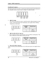
Page 28: ...thout turning the main power switch Off and then On Orientation is not required when making a connection to this header 1 RESET Pin Signal Name Reset 1 Reset 2 Ground IDE Hard Disk LED Connector This...

Page 29: ...pressed again it will force the SBC card to power off 1 PWR BTN Pin Signal Name Power 7 PWR BTN Button 8 GND CPU Fan Power Connector This is a 3 pin header for the CPU fan The fan must be a 12V fan 1...

Page 30: ...ost data 10 Host data 4 9 10 Host data 11 Host data 3 11 12 Host data 12 Host data 2 13 14 Host data 13 Host data 1 15 16 Host data 14 Host data 0 17 18 Host data 15 Ground 19 20 Key DRQ0 21 22 Ground...

Page 31: ...10 Host data 11 Host data 3 11 12 Host data 12 Host data 2 13 14 Host data 13 Host data 1 15 16 Host data 14 Host data 0 17 18 Host data 15 Ground 19 20 Key DRQ1 21 22 Ground Host IOW 23 24 Ground Hos...

Page 32: ...2 RM LC Ground 3 4 No connect Ground 5 6 No connect Ground 7 8 Index Ground 9 10 Motor enable 0 Ground 11 12 Drive select 1 Ground 13 14 Drive select 0 Ground 15 16 Motor enable 1 Ground 17 18 Direct...

Page 33: ...ine printer strobe 1 14 AutoFeed PD0 parallel data 0 2 15 Error PD1 parallel data 1 3 16 Initialize PD2 parallel data 2 4 17 Select PD3 parallel data 3 5 18 Ground PD4 parallel data 4 6 19 Ground PD5...

Page 34: ...dy 5 GND ground 6 DSR Data set ready 7 RTS Request to send 8 CTS Clear to send 9 RI Ring indicator 10 N C COM2 Serial Port COM2 a 10 pin header connector is the onboard COM2 serial port of the PISA E1...

Page 35: ...RTS Request to send 8 CTS Clear to send 9 RI Ring indicator 10 N C COM4 Serial Port COM4 a 10 pin header connector is the onboard COM4 serial port of the PISA E1 The following table shows its pin ass...

Page 36: ...bes the pin assignment of PS 2 Keyboard and Mouse connector which is mount on button of bracket To attach PS 2 Keyboard and mouse users need to connect trough a PS 2 1 to 2 Y cable and plug into this...

Page 37: ...please short pin3 4 together with a 2 54mm jumper cap 5V RX GND 1 TX RX OUT ISO_CAN Pin Signal Name 1 5V 2 TX 3 RX_IN 4 RX_OUT 5 GND CANBUS Connector There is CANBUS driver integrated on PISA E1 board...

Page 38: ...rm ATX power supply Soft on off function you have to connect the control signals and stand by power on this connector to your back plane by a corresponding cable Pin Signal Name 1 PWR_GD 2 5V_SB stand...

Page 39: ...K ACT STATUS ON Link OFF Disconnected FLASH Packets TX RX SPEED MODE ON 100Base T OFF 10Base T AT Power P8 Connector The following table describes the pin assignment of on board AT Power P8 connector...

Page 40: ...audio signals to the on board Audio CODEC 1 4 LAN LED Pin Signal Name 1 CD_Left 2 CD_AGND 3 CD_AGND 4 CD_Right Audio Connectors Audio connector is designed for wire the audio signals out from the on...

Page 41: ...PD14 29 30 FPD15 FPD16 31 32 FPD17 FPD18 33 34 FPD19 FPD20 35 36 FPD21 FPD22 37 38 FPD23 FPD24 39 40 FPD25 FPD26 41 42 FPD27 FPD28 43 44 FPD29 FPD30 45 46 FPD31 FPD32 47 48 FPD33 Part No OUPIIN 3215 5...

Page 42: ...FE VDD 5 6 EN_VDD VSYNC 7 8 EN_12V GND 9 10 DE DCLK 11 12 GND GND 13 14 GND 15 16 BLUE0 17 18 BLUE1 BLUE2 19 20 BLUE3 BLUE4 21 22 BLUE5 23 24 GREEN0 25 26 GREEN1 GREEN2 27 28 GREEN3 GREEN4 29 30 GREEN...

Page 43: ...D_4 23 24 RED_ EVEN _4 RED_ODD_5 25 26 RED_ EVEN _5 GREEN_ODD_0 27 28 GREEN_ EVEN _0 GREEN_ODD_1 29 30 GREEN_ EVEN _1 GREEN_ODD_2 31 32 GREEN_ EVEN _2 GREEN_ODD_3 33 34 GREEN_ EVEN _3 GREEN_ODD_4 35 3...

Page 44: ...t I O port 0443H To enable the watchdog timer and allow the system to reset read I O port 0443H To disable the timer read I O port 043H for the system to stop the watchdog function The timer has a tol...

Page 45: ...pics covered in this chapter are as follows BIOS Introduction 38 Main Menu 41 Standard CMOS Setup 43 Advanced BIOS Features 48 Advanced Chipset Features 52 Integrated Peripherals 57 Power Management S...

Page 46: ...ocess of configuring your system using Setup Starting Setup The AwardBIOS is immediately activated when you first power on the computer The BIOS reads the system information contained in the CMOS and...

Page 47: ...el menu Move Enter Move to the item you desired PgUp key Increase the numeric value or make changes PgDn key Decrease the numeric value or make changes key Increase the numeric value or make changes k...

Page 48: ...our computer no longer is able to boot the AwardBIOS supports an override to the CMOS settings which resets your system to its defaults The best advice is to only alter settings which you thoroughly u...

Page 49: ...gurations PC Health Status Frequency Voltage Control Load Fail Safe Defaults Load Optimized Defaults Set Supervisor Password Set User Password Save Exit Setup Exit Without Saving Esc Quit Select Item...

Page 50: ...ings for frequency voltage control Load Fail Safe Defaults Use this menu to load the BIOS default values for the minimal stable performance for your system to operate Load Optimized Defaults Use this...

Page 51: ...m Phoenix AwardBIOS CMOS Setup Utility Standard CMOS Features Date Mon Feb 8 2002 Time 16 19 20 IDE Primary Mast ST313620A IDE Primary Slave None IDE Secondary Master ATAPICDROM IDE Secondary Slave No...

Page 52: ...enter the sub menu of detailed options IDE Secondary Master Options are in its sub menu Press Enter to enter the sub menu of detailed options Drive A Drive B None 360K 5 25 in 1 2M 5 25 in 720K 3 5 in...

Page 53: ...IDE HDD Auto Detection Press Enter IDE Primary Master Auto Access Mode Auto Capacity 13667 MB Cylinder 26480 Head 16 Precomp 0 Landing Zone 26479 Sector 63 Item Help Menu Level To auto detect the HDD...

Page 54: ...5 means NONE Capacity Auto Display your disk drive size Disk drive capacity Approximated Note that this size is usually slightly greater than the size of a formatted disk given by a disk checking prog...

Page 55: ...0 column mode CGA 80 Power up in 80 column mode MONO For Hercules or MDA adapters Halt On This field determines whether the system will halt if an error is detected during power up No errors The syste...

Page 56: ...c 250 Security Option Setup OS Select For DRAM 64MB Non OS2 Video BIOS Shadow Enabled Item Help Menu Level Allows you to choose the VIRUS warning feature for IDE Hard Disk boot sector protection If th...

Page 57: ...k Power On Self Test This category speeds up Power On Self Test POST after you power up the computer If it is set to Enable BIOS will shorten or skip some check items during POST Enabled Enable quick...

Page 58: ...e when you hold the key down The choice 6 8 10 12 15 20 24 30 Typematic Delay Msec Sets the delay time after the key is held down before it begins to repeat the keystroke The choice 250 500 750 1000 S...

Page 59: ...The choice Non OS2 OS2 Video BIOS Shadow This item allows you to change the Video BIOS location from ROM to RAM Video Shadow will increase the video speed The choice Enabled Disabled C8000 CBFFF Shad...

Page 60: ...he specific features of the installed chipset This chipset manages bus speeds and access to system memory resources such as DRAM and the external cache It also coordinates communications between the c...

Page 61: ...en synchronous DRAM is installed the number of clock cycles of CAS latency depends on the DRAM timing Do not reset this field from the default value specified by the system designer The Choice 2 3 Mem...

Page 62: ...32M 65M 128M 256M Panel Type Select the panel type This BIOS pre configure several Panel parameters for your selection Call your dealer if you need customized BIOS to support your special Panel PANEL...

Page 63: ...T mode This selection help BIOS provide the information to OS what kind power supply the system use The correct information provide to OS can avoid the Windows Shutdown issue The Choice AT ATX OnChip...

Page 64: ...nfiguration 56 PISA E1 User s Manual OnChip Sound This should be Auto if your system will use on board Audio features If select disable it will disable on board Audio controller and AC97 codec The cho...

Page 65: ...Port 1 3F8 IRQ4 Onboard Serial Port 2 2F8 IRQ3 UART 2 Mode Standard X IR Function Duplex Half X TX RX inverting enable No Yes Item Help Menu Level Move Enter Select PU PD Value F10 Save ESC Exit F1 Ge...

Page 66: ...le only if your IDE hard drive supports it and the operating environment includes a DMA driver Windows 95 OSR2 or a third party IDE bus master driver If your hard drive and your system software both s...

Page 67: ...RX inverting which depends on different H W requirement This field is not recommended to change its default setting for avoiding any error in your system The Choice No No No Yes Default Yes No Yes Yes...

Page 68: ...type 1 7 or 1 9 The choice EPP1 7 1 9 Onboard Serial Port 3 Port 4 Select an address for the third and fourth serial ports The choice 3F0 2F0 3E0 2E0 Disabled Serial Port 3 Port 4 Use IRQ Select a co...

Page 69: ...PM Yes Video Off Option Suspend Off Video Off Method V H SYNC Blank MODEM Use IRQ 3 Wake Up Events Press Enter Item Help Menu Level Move Enter Select PU PD Value F10 Save ESC Exit F1 General Help F5 P...

Page 70: ...disabled each of the ranges are from 1 min to 1 hr except for HDD Power Down which ranges from 1 min to 15 min and disable PM Control by APM When enabled an Advanced Power Management device will be a...

Page 71: ...e In effect the system remains alert for anything which occurs to a device which is configured as On even when the system is in a power down mode VGA When Enabled you can set the VGA awakens the syste...

Page 72: ...signals this by causing an IRQ to occur When the operating system is ready to respond to the request it interrupts itself and performs the service When set On activity will neither prevent the system...

Page 73: ...noop Disabled Assign IRQ For VGA Enabled Assign IRQ For USB Enabled Item Help Menu Level Default is Disabled Select Enabled to reset Extended System Configuration Data ESCD when you exit Setup if you...

Page 74: ...egacy ISA for devices compliant with the original PC AT bus specification PCI ISA PnP for devices compliant with the Plug and Play standard whether designed for PCI or ISA bus architecture The Choice...

Page 75: ...IOS CMOS Setup Utility PC Health Status Current CPU Temperature 52 C 125 F Current System Temp 35 C 95 F Current CPU FAN Speed 4500 RPM Vcore 1 65V 2 5V 2 49V 3 3V 3 32V 5V 5 01V 12V 12 25V Item Help...

Page 76: ...le disable auto detect DIMM PCI Clock Turning off the un used PCI and DRAM clock may help to EMI issue Since there is no PCI clock routing specification for PICMG backplane some system may have PCI ca...

Page 77: ...Fail Safe Defaults Y N N Pressing Y loads the BIOS default values for the most stable minimal performance system operations Load Optimized Defaults When you press Enter on this item you get a confirma...

Page 78: ...o press Esc to abort the selection and not enter a password To disable a password just press Enter when you are prompted to enter the password A message will confirm the password will be disabled Once...

Page 79: ...after you turn your system off The next time you boot your computer the BIOS configures your system according to the Setup selections stored in CMOS After saving the values the system is restarted ag...

Page 80: ...72 PISA E1 User s Manual Appendix I O Port Address Map Interrupt Request Lines IRQ POST Beep...

Page 81: ...0h 03Fh Interrupt Controller 1 040h 05Fh Timer 060h 06Fh Keyboard Controller 070h 07Fh Real Time Clock NMI 080h 09Fh DMA Page Register 0A0h 0BFh Interrupt Controller 2 0C0h 0DFh DMA Controller 2 0F0h...

Page 82: ...red The following table shows the IRQ used by the devices on the Industrial CPU Card Level Function IRQ0 System Timer Output IRQ1 Keyboard IRQ2 Interrupt Cascade IRQ3 Serial Port 2 IRQ4 Serial Port 1...

Page 83: ...ates that a video error has occurred and the BIOS cannot initialize the video screen to display any additional information This beep code consists of a single long beep followed by two short beeps The...

Reviews: