Chapter3 BIOS Configuration
PISA-E1 User’s Manual
53
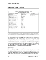
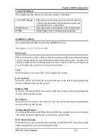
DRAM Timing By SPD
This item allows you to select the DRAM timing determined by the timing
information stored in SPD or set by the User manually. The default is Enabled.
When this field is set as Enabled, the DRAM Timing items below will become
read-only.
The Choice: Enabled, Disabled.
DRAM Clock .
This item allows you to select the related speed of SDRAM Memory bus. It chose
the HOST-33M and CPU FSB bus speed is 133MHz, the SDRAM will run on
100MHz. This allows system memory bus runs on different speed with CPU FSB
bus.
The Choice: HOST CLK, HCLK-33M, HCLK+33M
SDRAM Cycle Length
When synchronous DRAM is installed, the number of clock cycles of CAS
latency depends on the DRAM timing. Do not reset this field from the default
value specified by the system designer.
The Choice: 2, 3.
Memory Hole
In order to improve performance, certain space in memory is reserved for ISA
cards. This memory must be mapped into the memory space below 16MB.
The Choice: 15M-16M, Disabled.
System BIOS Cacheable
Selecting
Enabled
allows caching of the system BIOS ROM at F0000h-FFFFFh,
resulting in better system performance. However, if any program writes to this
memory area, a system error may result.
The choice: Enabled, Disabled.
Video RAM Cacheable
Select Enabled allows caching of the video RAM , resulting in better system
performance. However, if any program writes to this memory area, a system
error may result.
The Choice: Enabled, Disabled.


