xr
PRELIMINARY
XRT86VL38
REV. P1.0.6
OCTAL T1/E1/J1 FRAMER/LIU COMBO
132
T
ABLE
48: T
RANSMIT
I
NTERFACE
C
ONTROL
R
EGISTER
- E1 M
ODE
R
EGISTER
31 - E1 M
ODE
T
RANSMIT
I
NTERFACE
C
ONTROL
R
EGISTER
(TICR) H
EX
A
DDRESS
:0
X
n120
B
IT
F
UNCTION
T
YPE
D
EFAULT
D
ESCRIPTION
-O
PERATION
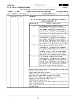
7
TxSyncFrD
R/W
0
Transmit Synchronous fraction data interface
This READ/WRITE bit-field selects whether TxCHCLK or TxSERCLK
will be used for fractional data input if the transmit fractional interface is
enabled. If TxSERCLK is selected to clock in fractional data input,
TxCHCLK will be used as an enable signal
0 = When this bit is set to ‘0’, fractional data Is clocked into the chip
using TxChCLK if the transmit fractional data interface is enabled.
1 = When this bit is set to ‘1’, fractional data is clocked into the chip
using TxSerClk if the transmit fractional data interface is enabled.
TxChClk is used as fractional data enable.
N
OTE
: The Time Slot Identifier Pins (TxChn[4:0]) still indicates the time
slot number if the transmit fractional data interface is not enabled. Frac-
tional Interface can be enabled by setting TxFr2048 to 1
6
Reserved
-
-
Reserved
5
TxPLClkEnb
R/W
0
Transmit payload clock enable
This READ/WRITE bit-field configures the E1 framer to output a regular
clock or a payload clock on the transmit serial clock (TxSERCLK) pin
when TxSERCLK is configured to be an output.
0 = Setting this bit to ‘0’ will configure the framer to output a 2.048MHz
clock on the TxSERCLK pin when TxSERCLK is configured as an out-
put.
1 = Setting this bit to ‘1’ will configure the framer to output a 2.048MHz
clock on the TxSERCLK pin when transmitting payload bits. There will
be gaps on the TxSERCLK output pin when transmitting overhead bits.
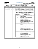
4
TxFr2048
R/W
0
Transmit Fractional/Signaling Interface Enabled
This READ/WRITE bit-field is used to enable or disable the transmit
fractional data interface, signaling input, as well as the 32MHz transmit
clock and the transmit overhead Signal output. This READ/WRITE bit-
field only functions when the device is configured in non-high speed or
multiplexed modes of operations.
If the device is configured in base rate:
0 = Setting this bit to ‘0’ will configure the 5 time slot identifier pins
(TxChn[4:0]) to output the channel number as usual.
1 = Setting this bit to ‘1’ will configure the 5 time slot identifier pins
(TxChn[4:0]) into the following different functions:
TxChn[0] becomes the Transmit Serial SIgnaling pin (TxSIG_n) for sig-
naling inputs. Signaling data can now be input from the TxSIG pin if
configured appropriately.
TxChn[1] becomes the Transmit Fractional Data Input pin (TxFrTD_n)
for fractional data input. Fractional data can now be input from the
TxFrTD pin if configured appropriately.
TxChn[2] becomes the 32 MHz transmit clock output
TxChn[3] becomes the Transmit Overhead Signal which pulses high on
the first bit of each multi-frame.
N
OTE
: This READ/WRITE bit-field has no function in the high speed or
multiplexed modes of operation


