XRT86VL38
PRELIMINARY
xr
OCTAL T1/E1/J1 FRAMER/LIU COMBO
REV. P1.0.6
77
1
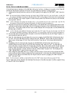
Encode AMI/B8ZS
R/W
0
Encode AMI or B8ZS/HDB3 Line Code Select
This READ/WRITE bit field enables or disables the B8ZS/HDB3
encoder on the transmit path.
0 = Setting this bit to ‘0’ will enable the B8ZS encoder for DS1 or HDB3
encoder for E1
1 = Setting this bit to ‘1’ will disable the B8ZS encoder for DS1 or HDB3
encoder for E1. When B8ZS/HDB3 encoder is disabled, AMI line code
is used.
0
Decode AMI/B8ZS
R/W
0
Decode AMI or B8ZS/HDB3 Line Code Select
This READ/WRITE bit field enables or disables the B8ZS/HDB3
decoder on the receive path.
0 = Setting this bit to ‘0’ will enable the B8ZS decoder for DS1 or HDB3
decoder for E1
1 = Setting this bit to ‘1’ will disable the B8ZS decoder for DS1 or HDB3
decoder for E1.
T
ABLE
13: G
ENERAL
P
URPOSE
I
NPUT
/O
UTPUT
0 C
ONTROL
R
EGISTER
R
EGISTER
2
A
G
ENERAL
P
URPOSE
I
NPUT
/O
UTPUT
0 C
ONTROL
R
EGISTER
(GPIOCR0) H
EX
A
DDRESS
: 0
X
0102
B
IT
F
UNCTION
T
YPE
D
EFAULT
D
ESCRIPTION
-O
PERATION
7
GPIO0_3DIR
R/W
1
GPIO0_3 Direction
This READ/WRITE bit-field permits the user to define the General Pur-
pose I/O Pin, GPIO0_3 as either in Input pin or an Output pin, as
described below.
0 – Configures GPIO0_3 to function as an input pin.
1 – Configures GPIO0_3 to function as an output pin.
1.
If GPIO0_3 is configured to function as an input pin, then the
user can monitor the state of this input pin by reading out the
state of Bit 3 (GPIO0_3) within this register.
2.
If GPIO0_3 is configured to function as an output pin, then the
user can control the state of this output pin by writing the appro-
priate value into Bit 3 (GPIO0_3) within this register.
6
GPIO0_2DIR
R/W
1
GPIO0_2 Direction
This READ/WRITE bit-field permits the user to define the General Pur-
pose I/O Pin, GPIO0_2 as either in Input pin or an Output pin, as
described below.
0 – Configures GPIO0_2 to function as an input pin.
1 – Configures GPIO0_2 to function as an output pin.
1.
If GPIO0_2 is configured to function as an input pin, then the
user can monitor the state of this input pin by reading out the
state of Bit 3 (GPIO0_2) within this register.
2.
If GPIO0_2 is configured to function as an output pin, then the
user can control the state of this output pin by writing the appro-
priate value into Bit 3 (GPIO0_2) within this register.
T
ABLE
12: L
INE
I
NTERFACE
C
ONTROL
R
EGISTER
R
EGISTER
1 - T1/E1 M
ODE
L
INE
I
NTERFACE
C
ONTROL
R
EGISTER
(LICR) H
EX
A
DDRESS
: 0
X
n101
B
IT
F
UNCTION
T
YPE
D
EFAULT
D
ESCRIPTION
-O
PERATION


