background image

FSD200

9

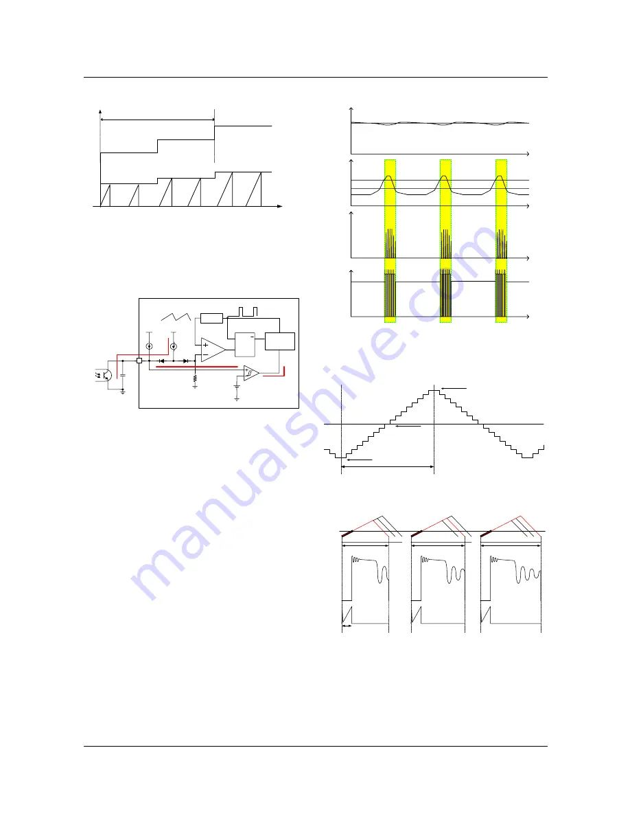
6. Burst operation :

 In order to minimize the power 

dissipation in standby mode, the FSD200/210 
implements burst mode. 

Figure 6. Circuit for burst operation

As the load decreases, the feedback voltage 
decreases. The device automatically enters burst mode 
when the feedback voltage drops below 0.5V. At this 
point switching stops and the output voltages start to 
drop. This causes the feedback voltage to rise. Once is 
passes 0.6V switching starts again. The feedback 
voltage falls and the process repeats. Burst mode 
operation alternately enables and disables switching of 
the power MOSFET to reduce the switching loss in the 
standby mode. 

Figure 7. Burst mode operation

7. Frequency Modulation

0.2A

0.25A

0.3A

3mS

Iover

FSD200/210

I(A)

t

OSC

4

Vfb

S

R

Q

GATE

DRIVER

5uA

250uA

0.6V

/0.5V

on/off

FSD2xx

Burst Operation Block

V

FB

Vds

0.5V

0.6V

Ids

Vo

Vo

set

time

130kHz

131kHz

132kHz

133kHz

134kHz

135kHz

136kHz

137kHz

138kHz

2mS

A

B

C

130kHz

134kHz

138kHz

Sawtooth

waveform

Ton

Vfb

Vdrain

Idrain

A

B

C

Summary of Contents for FSD200

Page 1: ...egrated PWM controller features A fixed oscillator with frequency modulation for reduced EMI Under voltage lock out Leading edge blanking LEB Optimized gate turn on turn off driver Thermal shut down p...

Page 2: ...rload protection OLP There is a time delay due to the 5uA current source which prevents false triggering under transient conditions but still allows the protection mechanism to operate under true over...

Page 3: ...2 kHz 4 Feedback Source Current Ifb Vfb 0V 0 22 0 25 0 28 mA Maximum Duty Cycle Dmax Vfb 3 5V 60 64 68 Minimum Duty Cycle Dmin Vfb 0V 0 0 0 Supply Regulation High Voltage Vregh 7 V Supply Regulation L...

Page 4: ...100 125 O perating Current Temp O u tput Frequ enc y 0 0 2 0 4 0 6 0 8 1 1 2 25 0 25 50 75 100 125 Fos c Figure 3 Peak Current Limit vs Temp Figure 4 Feedback Source Current vs Temp Over Current 0 00...

Page 5: ...raphs are normalized at Ta 25 C Figure 7 On State Resistance vs Temp Figure 8 Breakdown Voltage vs Temp On_State_Resistance 0 0 2 0 4 0 6 0 8 1 1 2 1 4 1 6 1 8 2 40 25 0 25 50 75 100 125 Rds on Breakd...

Page 6: ...FSD200 6 Typical Circuit FSD200 Snubber Circuit PWM Feedback Circuit Load...

Page 7: ...r a short time after the MOSFET is turned on Figure 3 PWM and feedback circuit 4 Protection Circuit The FSD200 210 has 2 self protection functions over load protection OLP and thermal shutdown TSD Bec...

Page 8: ...erefore once Vfb reaches 3V the device is switching at maximum power At this point the 250uA current source is blocked and the 5uA source continues to charge Cfb Once Vfb reaches 4V switching stops Th...

Page 9: ...tage to rise Once is passes 0 6V switching starts again The feedback voltage falls and the process repeats Burst mode operation alternately enables and disables switching of the power MOSFET to reduce...

Page 10: ...c ific a tio n W in d in g s p e c ific a tio n 4 4 E le c tric a l c h a ra c te ris tic E le c tric a l c h a ra c te ris tic IN S U L A T IO N P O L Y E S T E R T A P E t 0 0 2 5 m m 1 0 m m 3 T s...

Page 11: ...ND R1 100 D1 UF4004 R3 750 C3 47uF 25V U1 FSD20x 8 5 7 1 4 2 3 Vstr Vcc Drain GND Vfb GND GND D2 UF4004 1 1 1 2 Quantity 0 5A 700V 12V 0 5W Ic 200mA Vce 40V 1A 1000V Ultra Fast Diode Description Iover...

Page 12: ...FSD200 12 Package Dimensions 7 DIP...

Page 13: ...FSD200 13 Ordering Information Product Number Package Rating Topr C FSD200 7DIP 700V 0 5A 25 C to 85 C...

Page 14: ...nstructions for use provided in the labeling can be reasonably expected to result in a significant injury of the user 2 A critical component in any component of a life support device or system whose f...

Reviews: