GPS-RECEIVER JP7-T
VERSION 1.02
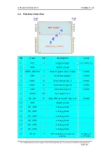
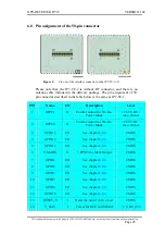
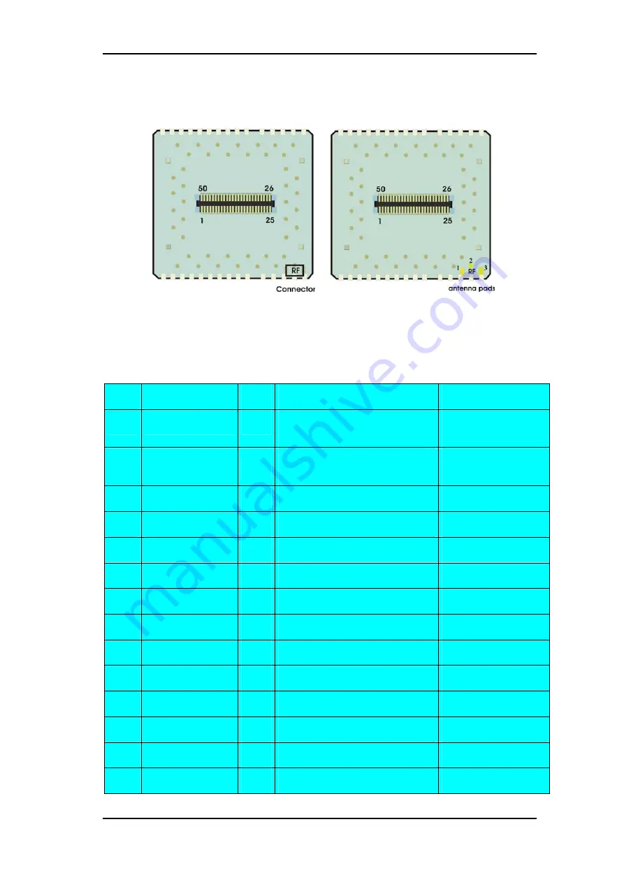
6.8 Pin assignment of the 50-pin connector
Figure 5:
Pin out of the interface connector on the JP7-TC-1(-2)
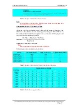
Please note that, the JP7-TC-2 is without RF connector, and there is no
antenna cable included in the delivery package. The pin assignment of 50-
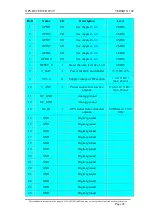
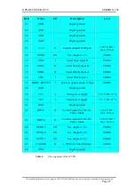
pin connector described in the table below is the same as JP7-TC-1.
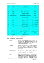
PIN
Name
I/O
Description
Level
1
RFPC1
O
Control output for Trickle-
Power Mode
+ 2.85 V DC /
max. 25 mA
2
RFPC0
O
Control output for Trickle-
Power Mode
+ 2.85 V DC /
max. 25 mA
3
GPIO15
I/O
CMOS
4
GPIO14
I/O
CMOS
5
GPIO13
I/O
CMOS
6
T-MARK
O
1 PPS Time Mark Output
CMOS
7
GPIO1
I/O
CMOS
8
GPIO0
I/O
CMOS
9
GPIO7
I/O
CMOS
10
GPIO5
I/O
CMOS
11
GPIO6
I/O
CMOS
12
GPIO10
I/O
CMOS
13
RESET_N
I
Reset the unit if Active Low
CMOS
14
V_BAT
I
Power for RTC and SRAM
+3 V DC ±5%
This confidential document is the property of FALCOM GmbH and may not be copied or circulated without permission.
Page 28


