
GPS-RECEIVER JP7-T
VERSION 1.02
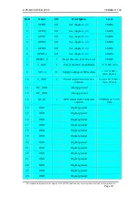
PIN
Name
I/O
Description
Level
40
SDI2
I
Serial Data Input B
CMOS
41
SDO2
O
Serial Data Output B
CMOS
42
SDO1
O
Serial Data Output A
CMOS
43
SDI1
I
Serial Data Input A
CMOS
44
BOOT_SELECT
I
Boots in update mode, if high
CMOS
45
VCC
I
Main power supply
+ 3.3 V DC
±
5 %
46
VCC
I
Main power supply
+ 3.3 V DC
±
5 %
47
VCC
I
Main power supply
+ 3.3 V DC
±
5 %
48
VCC
I
Main power supply
+ 3.3 V DC
±
5 %
49
VCC
I
Main power supply
+ 3.3 V DC
±
5 %
50
VCC
I
Main power supply
+ 3.3 V DC
±
5 %
Antenna pads on the JP7-TC-2, only
1
RF_GND
-
Analog ground
-
2
RF_IN
I
GPS signal from connected
antenna
50 Ohms @ 1.575
GHz
3
RF_GND
-
Analog ground
-
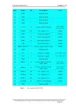
Table 6:
Pin assignment of the JP7-TC-1(-2)
6.8.1 Configuration and timing signals
RESET_N
This pin provides an active-low reset input to the
board. It causes the board to reset and to start
searching for satellites. Reset is an optional input
and, if not utilized, it may be left open.
T-MARK
This pin provides 1 pulse per second output from
the board, which is synchronized to within 1
microsecond of GPS time. The output is a CMOS
level signal.
BOOT_SELECT
Set this Pin to high (+3.3 V DC) for
reprogramming the flash of the JP7-T (for instance
updating a new firmware for the JP7-T ).
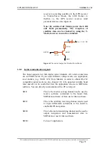
RFPC0
RFPC0 pin is provided to the JP7-TB and JP7-TC
module. This pin is a control output for the Trickle-
Power Mode. A possible circuit is shown in figure
below. If the LED lights permanently the GPS
This confidential document is the property of FALCOM GmbH and may not be copied or circulated without permission.
Page 30








![Navig[8]r NAVBIKE-GPS User Manual preview](http://thumbs.mh-extra.com/thumbs/navig-8-r/navbike-gps/navbike-gps_user-manual_3574097-01.webp)


