GPS-RECEIVER JP7-T
VERSION 1.02
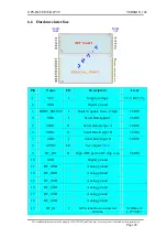
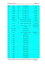
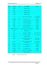
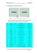
6.8.3 DC input signals
VCC
This is the main DC power supply for 3,3 V
powered board JP7-T family.
RF_IN
Active antennas have an integrated low-noise
amplifier. They can be directly connected to this
pin (
RF_IN)
. If an active antenna is connected to
RF_IN
, the integrated low-noise amplifier of the
antenna needs to be supplied with the correct
voltage through pin
V_ANT
.
C
aution:
Do not connect or disconnect the
antenna when the JP7-T family is running.
Caution:
The RF_IN is always fed from the input
voltage on the V_ANT. Do not use any input
voltage on this pin
V_ANT
This pin is an input and reserved for an external
DC power supply for an active antenna.
The antenna bias for an external active antenna can
be provided in two way to pin
V_ANT
.
In order to use a 5 V or 12 V active GPS antenna,
the
V_ANT
has to be connected to 5 V, 12 V
external power supply respectively.
The other possibility is available when you connect
the
VC3.0
output (which provides 3.0 V) to
V_ANT
,
so that an antenna with 3.0 V supply
voltage can be used.
Hint: The input voltage on the
V_ANT
should be
chosen in according to the antenna to be used.
Note: The GPS receiver JP7-T family has to be
connected with an active 3 V GPS antenna
(max. current of 25 mA). The antenna voltage is
provided by the internal power management.
VC3.0
This pin is an output which pr3.0 V DC,
and can be connected to the V_ANT, to supply the
connected GPS antenna. In Trickle Operation and
Push-To-Fix operation, VC3.0 is switched off
when the receiver sets itself into the sleep mode.
When the receiver wakes up the VC3.0 is switched
on.
This confidential document is the property of FALCOM GmbH and may not be copied or circulated without permission.
Page 32


