background image

GPS-RECEIVER JP7-T 

VERSION 1.02 

Hex 

ASCII 

Name 

Description 

0 x 1D 

29 

Nav. Lib. DGPS Data 

Differential GPS Data 

0 x 1E 

30 

Nav. Lib. SV State Data 

Satellite State Data 

0 x 1F 

31 

Nav. Lib. Initialization Data 

Initialization Data 

0 x FF 

255 

Development Data 

Various status messages 


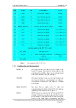
Table 7:


SiRF Output Messages


Table 8:  lists the message list for the SiRF input messages. 


Hex 

ASCII 

Name 

Description 

0 x 55 

85 

Transmit Serial Message 

User definable message 

0 x 80 

128 

Initialize Data Source 

Receiver initialization and 

associated parameters 

0 x 81 

129 

Switch to NMEA Protocol  Enable NMEA message, output rate 

and baud rate 

0 x 82 

130 

Set Almanac (upload) 

Sends an existing almanac file to the 

receiver 

0 x 84 

132 

Software Version (Poll) 

Polls for the loaded software version

0 x 85 

133 

DGPS Source Control 

DGPS correction source and beacon 

receiver information 

0 x 86 

134 

Set Main Serial Port 

Baud rate, data bits, stop bits and 

parity 

0 x 87 

135 

Switch Protocol 

Obsolete 

0 x 88 

136 

Mode Control 

Navigation mode configuration 

0 x 89 

137 

DOP Mask Control 

DOP mask selection and parameters

0 x 8A 

138 

DGPS Mode 

DGPS mode selection and timeout 

value 

0 x 8B 

139 

Elevation Mask 

Elevation tracking and navigation 

masks 

0 x 8C 

140 

Power Mask 

Power tracking and navigation 

masks 

0 x 8D 

141 

Editing Residual 

Not implemented 

0 x 8E 

142 

Steady-State Detection – not 

used 

Not implemented 

This confidential document is the property of FALCOM GmbH and may not be copied or circulated without permission. 

Page 35 

Summary of Contents for JP7-T Series

Page 1: ...This document is available at HTTP WWW FALCOM DE JP7 T Family GPS Receiver Hardware description Version 1 02...

Page 2: ...ECEIVER ARCHITECTURE 19 6 2 DESCRIPTION OF GPS RECEIVING SIGNALS 20 6 3 START UP MODES 20 6 3 1 Cold start 20 6 3 2 Warm start 21 6 3 3 Hot start 21 6 4 PRODUCT APPLICATIONS 21 6 5 TECHNICAL SPECIFICA...

Page 3: ...1 SiRFXTrac2 firmware default settings 49 11 4 2 Order options 50 Version history Version number Author Changes 1 00 Fadil Beqiri Initial version 1 01 Fadil Beqiri The signal names of serial ports upd...

Page 4: ...M and its range of products is available at the following internet address http www falcom de Trademarks Some mentioned products are registered trademarks of their respective companies Copyright The J...

Page 5: ...ty of frequency it offers a high improved performance Additionally a TCXO accept the condition for use the SiRFXTrac2 firmware The JP7 T family using SiRFXTrac2 firmware is able to track the GPS signa...

Page 6: ...7 T JP7 TB JP7 TC 1 JP7 TC 2 RF Part TCXO 25 5535 MHz 25 5535 MHz 25 5535 MHz 25 5535 MHz Active antenna power control built in built in built in built in RF connector Not available Not available U FL...

Page 7: ...SDI Data input SDO Data output SA Selective Availability WAAS Wide Area Augmentation System MSK Minimum Shift Keying PCB Printed Circuit Board PRN Pseudo random noise IF Intermediate Frequency A D An...

Page 8: ...option of JP7 T family imaged below please print this page with a colour printer The table below contains the order options of JP7 T family Name Options JP7 T 30 pin out on the left and right side of...

Page 9: ...aboratories etc Follow these instructions 1 3 Children Do not allow children to play with the GPS receiver It is not a toy and children could hurt themselves or others The GPS receiver consists of man...

Page 10: ...tions are recommended Protective outer garments Handle device in ESD safeguarded work area Transport device in ESD shielded containers Monitor and test all ESD protection equipment Treat the JP7 T fam...

Page 11: ...tection of public exposure to RF electromagnetic energy established by government bodies and professional organizations such as directives of the European Community Directorate General V in matters of...

Page 12: ...ilt in as well The digital baseband demodulator takes the quantified GPS signal and detects the individual satellites serial data bit stream along with the associated pseudo range This action consists...

Page 13: ...0 baud Msg GLL GGA RMC VTG GSV GSA 8 data bits no parity 1 stop bit SDI2 SDO2 RTCM 9600 baud trickle power mode The default Mode of FALCOM JP7 T is continuous Mode but the user can set FALCOM JP7 T in...

Page 14: ...pprox 95 approx 15 mW ca 4 8 mA at Vcc 3 3 V For more details see chapter 4 Operating modes Figure 2 Example for the trickle power mode of FALCOM JP7 T family This confidential document is the propert...

Page 15: ...s preferable to be connected to an external back up battery so that the RTC is running during the power interrupt The backup power is required for retention of SRAM memory and maintaining the Real Tim...

Page 16: ...ing calibrated The transition into the Push to Fix mode of JP7 T family can be implemented and configured by using the Set Operating Mode command in SiRFdemo During the subsequent background cycles or...

Page 17: ...late the Trickle Power update rate as a function of Duty Cycle and On Time use the following formula On Time Duty Cycle On Time Off Time Duty Cycle Update rate Off Time On Time Hint It is not possible...

Page 18: ...1800 seconds Comparison A comparison of the Trickle Power and Push to Fix modes is shown in Figure below This diagram shows that for position update intervals less than approximately 600 seconds i e...

Page 19: ...I architecture builds on the high performance SiRFstarI core adding an acquisition accelerator differential GPS processor multipath mitigation hardware and satellite tracking engine The JP7 T family d...

Page 20: ...the JP7 T family depend on the last stored position in the SRAM memory such as the current time and ephemeris data So that the JP7 T family can be initiated to one of three different start up procedu...

Page 21: ...ime clock RTC has been operating during that switch off time This start up procedure performs computing of valid positions only The problems which may be met while start up modes The validity of the R...

Page 22: ...5 sec average Cold start 45 sec average The values listed above are available by using the SiRFXTrac2 firmware only 6 5 1 6 Sensitivity Tracking 16 dBHz Hot Start 23 dBHz Warm Start 28 dBHz Cold Start...

Page 23: ...V RMC and VTG DGPS protocol RTCM SC 104 version 2 32 type 1 5 and 9 6 5 1 11 Time 1PPS Pulse Level CMOS Pulse duration 100 ms Time reference At the pulse positive edge Measurements Aligned to GPS seco...

Page 24: ...ta Output B CMOS 7 SDI2 I Serial Data Input B CMOS 8 GPIO3 I O See chapter 6 8 4 9 RF_ON O High if RF part on RF chip is on CMOS 10 GND Digital ground 11 RF_GND Analog ground 12 RF_GND Analog ground 1...

Page 25: ...ction 3 0 V DC 21 V_BAT I Power for RTC and SRAM 3 V DC 5 22 RESET_N I Resets the unit if active LOW CMOS 23 GPIO10 I O See chapter 6 8 4 CMOS 24 GPIO6 I O See chapter 6 8 4 CMOS 25 GPIO5 I O See chap...

Page 26: ...0 V DC max 25 mA 10 V_ANT I Power supply for an active antenna Up to 12 V DC max 25 mA 11 RF_GND Analog ground 12 RF_GND Analog ground 13 RF_IN I GPS signal from connected antenna 50 Ohms 1 575 GHz 14...

Page 27: ...update mode if high CMOS 38 GND Digital ground 39 VCC I Main power supply 3 3 V DC 5 30 VCC I Main power supply 3 3 V DC 5 41 GND Digital ground 42 RFPC1 O Control output for Trickle Power Mode 2 85 V...

Page 28: ...mA 2 RFPC0 O Control output for Trickle Power Mode 2 85 V DC max 25 mA 3 GPIO15 I O See chapter 6 8 4 CMOS 4 GPIO14 I O See chapter 6 8 4 CMOS 5 GPIO13 I O See chapter 6 8 4 CMOS 6 T MARK O 1 PPS Time...

Page 29: ...C max 25 mA 21 GND Digital ground 22 V_ANT I Power supply for an active antenna Up to 12 V DC max 25 mA 23 GND Digital ground 24 GND Digital ground 25 GND Digital ground 26 GND Digital ground 27 GND D...

Page 30: ...7 TC 1 2 6 8 1 Configuration and timing signals RESET_N This pin provides an active low reset input to the board It causes the board to reset and to start searching for satellites Reset is an optional...

Page 31: ...te level shifters e g MAX 3232 from Maxim in order to obtain RS 232 compatible signal levels se also chapter 10 All supported variable baud rates and all can be controlled from the appropriate screens...

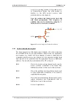
Page 32: ..._ANT In order to use a 5 V or 12 V active GPS antenna the V_ANT has to be connected to 5 V 12 V external power supply respectively The other possibility is available when you connect the VC3 0 output...

Page 33: ...e CPU are connected to the hardware interface connector of the JP7 T family They are reserved for customer specific applications For example For realization a SPI Bus For realization an Antenna indica...

Page 34: ...x 07 7 Clock Status Current clock status 0 x 08 8 50 BPS Subframe Data Standard ICD format 0 x 09 9 Throughput Navigation complete data 0 x 0A 10 Error ID Error coding for message failure 0 x 0B 11 C...

Page 35: ...d Sends an existing almanac file to the receiver 0 x 84 132 Software Version Poll Polls for the loaded software version 0 x 85 133 DGPS Source Control DGPS correction source and beacon receiver inform...

Page 36: ...ush to fix mode duty cycle and on time 0 x 98 152 Poll Navigation Parameters Polls for the current navigation parameters 0 x A5 165 Set UART Configuration Protocol selection baud rate data bits stop b...

Page 37: ...TG Course and speed information relative to the ground Table 9 NMEA Output Messages 7 2 2 NMEA input messages Message MID1 Description Set Serial Port 100 Set PORT A parameters and protocol Navigation...

Page 38: ...not printable ASCII characters they are omitted from the example strings but must be sent to terminate the message and cause the receiver to process that input message CheckSum The checksum is 15 bit...

Page 39: ...T JP7 TB JP7 TC 1 JP7 TC 2 is 25 4 mm x 25 4 mm L x B Figure 7 shows the top view on JP7 T family without connectors and provides an overview of the mechanical dimensions of the board Please note tha...

Page 40: ...20 mm 4 20 mm 3 70 mm 1 70 mm 23 70 mm 5 70 mm 6 70 mm 8 20 mm 11 20 mm 12 70 mm 14 20 mm 15 70 mm 17 20 mm 18 70 mm 19 70 mm 3 20 mm 1 70 mm 22 20 mm 22 70 mm 21 20 mm 21 70 mm 2 70 mm 9 70 mm 20 70...

Page 41: ...tor 21 7 mm 12 7 mm 12 7 mm 1 67 mm Figure 9 The mechanical draw of the JP7 TC 1 1 25 26 50 RF antenna pads 12 7 mm 12 7 mm 1 67 mm 1 70 mm O 1 00 mm 1 05 mm 2 20 mm Round ball Square pads for an ante...

Page 42: ...und plane of the JP7 T family GPS receiver 9 2 RF connection The JP7 T family GPS receiver is designed to be functional by using either a passive patch antenna or an antenna connector with standard RF...

Page 43: ...pin name refer also on the table 6 Figure 13 RF connection to antenna feed of the JP7 TC 2 GPS receiver Recommendations for layout and soldering Please note that the dimension tolerance is 0 1 mm 2 0...

Page 44: ...o prevent component and substrate damages Peak temperature must not exceed 240 C JP7 T family are able to withstand twice the previous recommended reflow profile in order to be compatible with a doubl...

Page 45: ...d connect the line which supply the VCC pin to 3 3 V properly If they are correctly connected a proper RESET signal is internally generated the board is full powered and the unit begins obtaining its...

Page 46: ...d up SRAM are continually supplied through V_BAT The voltage at this pin has to be 3 V DC 5 If you do not use a backup battery connect this pin to GND or leave it open Do not use a super cap for the b...

Page 47: ...software are available on the Falcom s Website for free download www falcom de service downloads manual SiRF SiRFdemo pdf www falcom de service downloads manual SiRF SiRFdemo zip This confidential doc...

Page 48: ...TC uses an ultra miniature SMT antenna connector supplied from Hirose Ltd The product name is U FL R SMT The position of the antenna connector on the JP7 TC board has to be seen on bottom side on the...

Page 49: ...the GPS signals an extremely small level by 16 dBHz While trying to calculate a position fix the receiver needs to be locked on to at least four satellites Your position can be extremely quick fixed w...

Page 50: ...nd right side of JP7 T are available for use JP7 TBX SiRFXTrac2 48 Balls are available for use JP7 TCX 1 SiRFXTrac2 A 50 pin connector and a RF connector are available for use JP7 TCX JP7 TCX 2 SiRFXT...

Reviews: