2007-11-19
Page 16 of 35
IT321_Tech_doc_12
4. CONNECTIVITY
4.1 Connection assignments
The I/O connections are available as soldering pads on the bottom
side of the module. These pads are also used to attach the module on
the motherboard in application. All unconnected I/O should be left
open (floating) unless instructed to use pull external up or pull down.
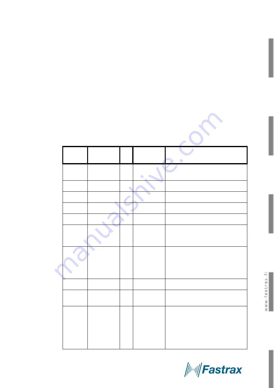
Table 5
Connections
Contact Signal
name
I/O Alternative
signal name
Signal description
1
ANT
I/O
-
Antenna signal input 50 ohm, An-
tenna bias v2.7V output
2 GND
- -
Ground
3 GND
- -
Ground
4 GND
- -
Ground
5 GND
- -
Ground
6
GPIO6
I
-
Control input for protocol configura-
tion. VCC=1.8V. For default pull
low.
7
ON_OFF
I
-
Interrupt toggle (pulse low-high-low
100ms) for switching between Hi-
bernate/Normal mode. VCC=1.2V.
Pull to low state with e.g. 10kohm if
not used.
8 GND
- -
Ground
9
VDD
-
-
Power supply, can be raw battery
voltage. Note ripple voltage spec.
10
BOOT1
I
-
BOOT select 1. Can be left uncon-
nected with ROM version.
With flash version connect to
BOOT2 signal and pull low with
R<5kohm. Has internal pull down
resistor 100kohm. VCC=1.8V.
Summary of Contents for IT321
Page 15: ...2007 11 19 Page 15 of 35 IT321_Tech_doc_12 Figure 2 SiRFFlash utility settings...
Page 25: ...2007 11 19 Page 25 of 35 IT321_Tech_doc_12 Figure 7 Tape and reel specification...
Page 32: ...2007 11 19 Page 32 of 35 IT321_Tech_doc_12 7 3 Circuit drawing rev C...
Page 34: ...2007 11 19 Page 34 of 35 IT321_Tech_doc_12 7 6 Artwork layer 2 rev C 7 7 Artwork layer 3 rev C...
Page 35: ...2007 11 19 Page 35 of 35 IT321_Tech_doc_12 7 8 Artwork layer 4 Bottom rev C...


