background image

2010-06-30 

Page 18 of 42 

IT430_Tech_doc.doc


VDD supply ripple voltage: 54 mV(RMS) max @ f = 0… 3MHz 
and 15 mV(RMS) max @ f > 3 MHz. 


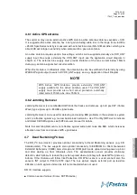
4.3  Host Port Configuration: RTS_N and CTS_N 

User  can  select  the  host  port  configuration  between  UART,  SPI  (slave)  and  I

2

C  (master/slave) 

during power up boot. At system reset, the host port  pins are disabled, so there will be no  port 
conflict occurring. Depending on the host port type, the software enables the correct port drivers, 
sets up the port hardware, configures the pins according to the port type and begins operations. 

The  port  selection  is  not  intended  to  be  changed  dynamically  but  only  set  once  at  power  up. 
Default host port is SPI (selected by internal pull up/down resistors that are present during power 
up) and other host port configurations requires connection of external pull down (to 0V) or pull up 
(to 1.8V) resistor at CTS_N and RTS_N pins, see table below. 

Table 4


Host port boot strap 

Host port 

RTS_N 

CTS_N 

UART 

Pull up 10 kohm 

SPI (default) 

I

2

Pull down 10 kohm 


4.3.1 Host Port UART 

UART is normally used for GPS data reports and receiver control. Serial data rates are selectable 
from  1200  baud  to  1.8432  Mbaud.  Default  baud  rate  is  4800  baud;  default  protocol  is  NMEA 
(switchable to SiRF OSP binary). RX signal must be driven by host or pulled up externally. 

4.3.2 Host Port SPI 

The host interface SPI is a slave mode SPI: 

 Supports both SPI and Microwire formats 

 An interrupt is provided when the transmit FIFO and output serial register (SR) are both empty 

 The transmitter and receiver each have independent 1024B FIFO buffers 

 The transmitter and receiver have individual software-defined 2-byte idle patterns 

 SPI detects synchronization errors and is reset by software 

 Supports a maximum clock of 6.8MHz. 

 A timer is provided to generate an interrupt when: 

Summary of Contents for IT430

Page 1: ...REV 1 5 TECHNICAL DESCRIPTION Fastrax IT430 OEM GPS Receiver This document describes the electrical connectivity and main functionality of the Fastrax IT430 OEM GPS Receiver June 30 2010 Fastrax Ltd ...

Page 2: ...e free of errors accurate or complete and therefore assumes no liability for loss or damage of any kind incurred directly or indirectly through the use of this document The information in this document is subject to change without notice and describes only generally the product defined in the introduction of this documentation Fastrax products are not authorized for use in life support or safety c...

Page 3: ...ated power consumption and added notes on internal regulator mode added note on ESD sensitivity of the antenna input added out of band RF_IN power spec to abs max 2010 05 11 1 3 Added chapter on reset state Clarified low power operation modes added APM notes on PTF SiRFAware 2010 06 04 1 4 Added two module variants corrected volatile data RAM clearing at reset added Tape Reel spec added chapter on...

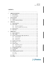
Page 4: ...1 3 2 2 Power management system modes 11 3 3 Hibernate state 12 3 4 Reset state 13 4 CONNECTIVITY 14 4 1 Signal assignments 14 4 2 Power supply 16 4 3 Host Port Configuration RTS_N and CTS_N 18 4 3 1 Host Port UART 18 4 3 2 Host Port SPI 18 4 3 3 Host Port I2 C 19 4 4 ON_OFF control input 19 4 5 Reset input 20 4 6 Antenna input 20 4 6 1 Active GPS antenna 21 4 6 2 Jamming Remover 21 4 7 Dead Recko...

Page 5: ...e sensitivity 27 5 3 Marking 27 5 3 1 Module variants 28 5 4 Tape and reel 29 6 REFERENCE DESIGN 30 6 1 Reference circuit diagram 30 6 2 PCB layout issues 31 7 IT430 APPLICATION BOARD 33 7 1 Card Terminal I O connector 33 7 2 Bill of materials 35 7 3 Circuit drawing 38 7 4 Assembly drawing Top side 39 7 5 Artwork layer 1 Top 39 7 6 Artwork layer 2 40 7 7 Artwork layer 3 40 7 8 Artwork layer 4 Bott...

Page 6: ...s are complementary reading for this document Ref File name Document name I SiRFstarIV Brochure pdf SiRFstar IV Brochure II CS 129435 MA N pdf NMEA Protocol Reference Manual III CS 129291 DC 2 pdf One Socket Protocol OSP Interface Control Document IV Reflow_soldering_ profile pdf Soldering Profile ...

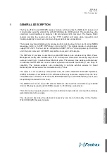
Page 7: ...r Management mode which enables fast TTFF for Snap start mode while consuming only 500 uA average current typ in autonomous Hibernate state The receiver does wakeup autonomously to calibrate internal GPS time and to collect ephemeris data while maintaining 1 sec Snap fix capability The module supports also connectivity to optional external sensors for Dead Reckoning like 3D accelerometer on dedica...

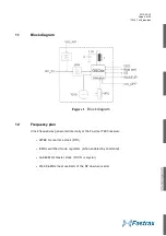
Page 8: ...ck diagram 1 2 Frequency plan Clock frequencies generated internally at the Fastrax IT430 receiver 32768 Hz real time clock RTC 8 MHz switched mode regulator when enabled by command 16 369 MHz master clock TCXO or crystal 3142 96 MHz local oscillator of the RF down converter ...

Page 9: ...re 40ºC 85ºC Operating temperature 40ºC 85ºC note 2 Host port configuration SPI default UART or I2 C Serial port protocol UART NMEA configurable to SiRF binary OSP Serial data format UART 8 bits no parity 1 stop bit Serial data speed UART 4800 baud configurable I O signal levels CMOS compatible low state 0 0 4 V max high state 0 75 1 0xVDD Inputs are 3 6 V tolerable I O output sink source capabili...

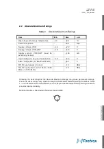
Page 10: ...t voltage on any input connection 0 3 3 6 V ESD voltage RF_IN Machine Model 50 V RF_IN input power in band 10 dBm RF_IN input power out of band 1460 MHz or 1710 MHz 15 dBm Stressing the device beyond the Absolute Maximum Ratings may cause permanent damage These are stress ratings only Operation beyond the Recommended Operating Conditions Table 1 is not recommended and extended exposure beyond the ...

Page 11: ...next power up VDD supply is intended to be kept active all the time and navigation activity is suggested to be controlled to low quiescent Hibernate state via ON_OFF control input See also chapter 3 3 and 4 2 3 2 1Host port configuration User can select the host port configuration between UART SPI slave and I 2 C master slave during power up boot The port selection is not intended to be changed dy...

Page 12: ...in The host wakes up the receiver by ON_OFF control input interrupt pulse low high low 90us to Full on power mode after which the receiver performs Snap start and a valid fix is available within 1 second typ After valid fix operation can return back to Micro Power Management mode by re sending the configuration binary message from host This mode is configurable with SiRF OSP One Socket Protocol bi...

Page 13: ...the internal RTC clock wakes up after which internal reset state is relaxed Host can override reset state via RESET_N pin 12 input low state active Normally external reset override is not required but if power shall be removed abruptly see chapter 4 2 for reset suggestion Note that reset clears data RAM content e g downloaded ROM patch code Backup RAM content is not cleared and thus fast TTFF is p...

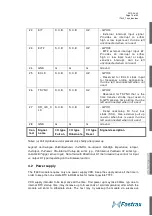
Page 14: ...ith e g 4 7uF low ESR ceramic capacitor 2 DR_I2C_D IO S C B S C B HZ GPIO0 Dead reckoning I2 C host bus data SDA Use external pull up resistor when bus is used Can be left unconnected when not used 3 VDD_ANT P I P I P I Antenna bias power supply input up to 5 5V De couple signal further externally see Application Circuit Diagram 4 GND G G G Ground 5 GND G G G Ground 6 RF_IN A I O A I O A I O Analo...

Page 15: ...UART RX I2C_DIO I C bus data SDA 17 ON_OFF S C B S C B S C B Power control input used to command the module On Navigation or Off Hibernate Must be driven by the host 18 GND G G G Ground 19 GND G G G Ground 20 TM S C B S C B HZ GPIO5 Time mark output signal default 1PPS Optionally GPS_ON power control output signal for e g external LNA bias control Optionally RTC_CLK buffered RTC clock output Can b...

Page 16: ...istor when bus is used Can be left unconnected when not used 28 GND G G G Ground Con tact Signal name I O type Full on I O type Hibernate I O type Reset Signal description Notes a Pull Up down resistor present only shortly after power up Legend A Analogue B Bidirectional C CMOS G Ground HZ High Impedance I Input O Output P Power PU Internal Pullup 86 kohm typ PD Internal Pulldown 91 kohm typ S Sch...

Page 17: ...current varies according to the processor load and satellite acquisition Typical VDD peak current is 56 mA typ during waking for Full on power up Typical VDD current in low power Hibernate state is 20uA The external power supply can be using dual low high current modes which can be controlled via the WAKEUP output signal high current WAKEUP high as indication when full power is required by the mod...

Page 18: ...of external pull down to 0V or pull up to 1 8V resistor at CTS_N and RTS_N pins see table below Table 4 Host port boot strap Host port RTS_N CTS_N UART Pull up 10 kohm SPI default I2 C Pull down 10 kohm 4 3 1 Host Port UART UART is normally used for GPS data reports and receiver control Serial data rates are selectable from 1200 baud to 1 8432 Mbaud Default baud rate is 4800 baud default protocol ...

Page 19: ... transmit and slave receive at the same time 4 4 ON_OFF control input The ON_OFF control input must be used by the host to wakeup the module after first power up and to control the receiver activity between Normal and Hibernate states and also to generate interrupt in Push to Fix and SiRFAware modes of operation The module will boot to Hibernate state after power up First ON_OFF interrupt wakes up...

Page 20: ... reset by means of external VDD voltage monitor When RESET_N signal is used it will force volatile RAM data loss e g ROM patch code Non Volatile Backup RAM content is not cleared and thus fast TTFF is possible after reset The input has internal pull up resistor 86 kohm typ and leave it not connected floating if not used 4 6 Antenna input The module supports passive and active antennas The antenna ...

Page 21: ...Jamming Remover Jamming Remover is an embedded HW block that tracks and removes up to 8 pcs CW Carrier Wave type signals up to 90 dBm signal levels Jamming Remover can be used for detecting and solving EMI problems in the customer s system and it is effective against e g narrow band clock harmonics Use PC utility SiRFLive to indicate and detect CW EMI signals see SiRFLive user manual for details N...

Page 22: ...nsition WAKEUP signal can be also used externally to switch off the Active Antenna Bias supply voltage VDD_ANT during Hibernate state polarity is active high VDD_ANT active 4 10 Interrupt inputs EIT and EIT2 The EIT and EIT2 are external level sensitive interrupt inputs EIT2 pin is also configurable as an edge sensitive input Both pins are disabled at initial power up and usage is configured by th...

Page 23: ... enough time for the RTC re timing process to sample the level 3 RTC_CLK ticks are sufficient about 90µs At system reset the EIT2 pin is disabled 4 11 ELCK The ECLK is reserved for external clock input with special variant for A GPS frequency aiding The input can be left not connected when not used 4 12 TSYNC TSYNC input is reserved for external time aiding with a special variant used for A GPS Th...

Page 24: ...2010 06 30 Page 24 of 42 IT430_Tech_doc doc Figure 3 Dimensions ...

Page 25: ...c Figure 4 I O pad numbering and dimensions bottom view 4 14 Test points On the bottom side of the module there are also test points TP1 TP8 which are reserved for production testing Leave these test points floating not connected and unsoldered ...

Page 26: ...2010 06 30 Page 26 of 42 IT430_Tech_doc doc 4 15 Suggested pad layout Figure 5 Suggested pad layout and occupied area top view Suggested paste mask openings equal pad layout ...

Page 27: ...Machine Model at RF_IN Avoid also ultrasonic exposure due to internal crystal and SAW components The IT430 module meets the requirements of Directive 2002 95 EC of the European Parliament and of the Council on the Restriction of Hazardous Substance RoHS For details contact Fastrax support 5 2 Moisture sensitivity IT430 module is moisture sensitive at MSL 3 see the standard IPC JEDEC J STD 020C The...

Page 28: ... 3 1 Module variants The IT430 module is available in two variants based on firmware feature set Note that by default IT430 is shipped with Signature feature set and Basic feature set variant is available only on request IT430 sssr BSC Basic feature set available only on request sssr FW revision o CW Jammer Remover o Embedded Client and Server generated EE support o TricklePower APM and Push to Fi...

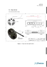
Page 29: ...2010 06 30 Page 29 of 42 IT430_Tech_doc doc 5 4 Tape and reel One reel contains 500 modules Figure 6 Tape and reel specification ...

Page 30: ...ignal can be used for external regulator mode control for full power state WAKEUP signal can be also used to drive external antenna bias VDD_ANT 3 3 V typ voltage switch Q1 during Normal Hibernate modes L1 and C2 provide Additional RF decoupling to VDD_ANT supply The host port is configured to UART by the pull up resistor R5 Serial port TX output is connected to host UART input RX input connection...

Page 31: ...sues The suggested 4 layer PCB build up is presented in the following table Table 5 Suggested PCB build up Layer Description 1 Signal RF trace Ground plane with solid copper under IT430 2 Ground plane for signals and for RF trace 3 Signals and power planes 4 Ground plane also short traces allowed ...

Page 32: ... as close as possible to the capacitor Connect the GND soldering pads of the IT430 to ground plane with short traces thermals to via holes which are connected to the ground plane Use preferably one via hole for each GND pad The RF input should be routed clearly away form other signals this minimizes the possibility of interference The proper width for the 50 ohm transmission line impedance depends...

Page 33: ...he following signals are available at the 40 pin Card Terminal I O connector J2 The same pin numbering applies also to the Fastrax Evaluation Kit pin header J4 Note that UART Port maps to serial Port 0 at the Fastrax Evaluation Kit I O signal levels are CMOS 3 3V compatible unless stated otherwise Table 6 IT430 Application Board connectivity Pin Signal name I O Alternative GPIO name Interface to F...

Page 34: ... 28 Not connected 29 Not connected 30 UI_A_3V3 O WAKEUP UI indicator A output VDD 3 3V 31 GND Ground 32 Not connected 33 GND Ground 34 Not connected 35 GND Ground 36 TSYNC I Timesync timing input VDD 1 8V 37 GND Ground 38 ECLK I ECLK clock input VDD 1 8V 39 GND Ground 40 ON_OFF_N I ON_OFF inv Inverted ON_OFF control input pulled up to VDD_3V3 Pin Signal name I O Alternative GPIO name Interface to ...

Page 35: ...4U7 6V3 T5P 4u7F 10 1 C4 C 0805 X5R 4U7 6V3 T5P 4u7F 11 1 C7 C 0805 X5R 4U7 6V3 T5P 4u7F 12 1 C11 C 0805 X5R 4U7 6V3 T5P 4u7F 13 1 H3 FIDUCIAL FIDUCIAL 14 1 H4 FIDUCIAL FIDUCIAL 15 1 H1 HOL M3 0 Hole M 3 0mm metallized 16 1 H2 HOL M3 0 Hole M 3 0mm metallized 17 1 A1 IT430_APP_TP IT430A01 18 1 J4 J 1X2 0 2P54 1x2P2 54 19 1 J6 J 1X2 0 2P54 1x2P2 54 20 1 J2 J 2X20 EDGE 2x20 edge 21 1 J3 J 2X5 2P54 2...

Page 36: ...kohm 5 39 1 R34 R 0402 1K5 T5P G N A 40 1 R35 R 0402 1K5 T5P G N A 41 1 R4 R 0402 220R 5P G 220R 5 42 1 R6 R 0402 220R 5P G 220R 5 43 1 R7 R 0402 220R 5P G 220R 5 44 1 R9 R 0402 220R 5P G 220R 5 45 1 R10 R 0402 220R 5P G 220R 5 46 1 R20 R 0402 220R 5P G 220R 5 47 1 R21 R 0402 220R 5P G 220R 5 48 1 R8 R 0402 33K 1P G 33k 1 49 1 R2 R 0402 47R T5P 47R 5 50 1 R3 R 0402 47R T5P 47R 5 51 1 R5 R 0402 47R...

Page 37: ... 5 62 1 R24 R 0402 47R T5P 47R 5 63 1 S1 S JMP 1X2 J4 P1 P2 64 1 S4 SW 2M54 SW JMP 2P54 65 1 S5 SW 2M54 SW JMP 2P54 66 1 S6 SW 2M54 SW JMP 2P54 67 1 S7 SW 2M54 SW JMP 2P54 68 1 S8 SW 2M54 SW JMP 2P54 69 1 S3 SW PUSHBUTTON SW 70 1 U5 U EEPROM M24M01 M24M01 RMN6TP 71 1 U2 U FXL4TD245 FXL4TD245 72 1 U4 U LOGIC NC7S14 NC7SZ14M5X 73 1 U3 U REG ADJ TPS79101 TPS79101 ...

Page 38: ...2010 06 30 Page 38 of 42 IT430_Tech_doc doc 7 3 Circuit drawing ...

Page 39: ...2010 06 30 Page 39 of 42 IT430_Tech_doc doc 7 4 Assembly drawing Top side 7 5 Artwork layer 1 Top ...

Page 40: ...2010 06 30 Page 40 of 42 IT430_Tech_doc doc 7 6 Artwork layer 2 7 7 Artwork layer 3 ...

Page 41: ...2010 06 30 Page 41 of 42 IT430_Tech_doc doc 7 8 Artwork layer 4 Bottom ...

Page 42: ...T430_Tech_doc doc Contact Information Fastrax Ltd Street Address Valimotie 7 01510 Vantaa FINLAND Tel 358 0 424 733 1 Fax 358 0 9 8240 9691 http www fastraxgps com E mail Sales sales fastraxgps com Support support fastraxgps com ...
Reviews: