background image

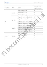
Pin
Number

Pin Name

I/O

Reset
Status

Pin Description

Type

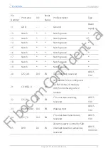
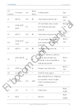
52

CLKREQ#

DIO

T

PCIe clock request signal, active
low, open drain output, an
external pull-up resistor needs
to be reserved

CMOS
3.3V/1.8V

53

REFCLKN

DIO

*

PCIe reference clock differential
negative signal

*

54

PEWAKE#

DO

T

PCIe wake-up signal, active low,
open drain output, an external
pull-up resistor is required

CMOS
3.3V/1.8V

55

REFCLKP

DIO

*

PCIe reference clock differential
positive signal

*

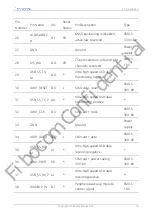
56

RFFE_SCLK

DO

PD

RFFE-MIPI serial clock signal,
I2C_SCL (Reserved)

CMOS
1.8V

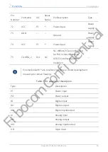
57

GND

- -

- -

Ground

Power
supply

58

RFFE_SDATA DIO

PD

RFFE-MIPI serial data signal,
I2C_SDA (Reserved)

CMOS
1.8V

59

GRFC7

DO

PD

A high level is output and the
5GHz WLAN LNAs is turned off
when the n79 transmitting
power exceeds 10dBm

CMOS
1.8V

60

COEX3/GPIO
86

DI

*

Output a high level to the
module to turn off the n79 LNAs
when the external 5 GHz WLAN
transmitting power exceeds a
certain threshold

CMOS
1.8V

3. Pin Definition

Copyright © Fibocom Wireless Inc.

18

Fibocom Confidential

Summary of Contents for FM101-NA-20

Page 1: ...FM101 NA 20 Hardware Guide V1 0 F i b o c o m C o n f i d e n t i a l...

Page 2: ...rsion upgrade or other reasons Unless otherwise specified the document only serves as the user guide All the statements information and suggestions contained in the document do not constitute any expl...

Page 3: ...ock Diagram 10 2 5 Evaluation Board 12 3 Pin Definition 13 3 1 Pin Distribution 13 3 2 Pin Function 14 4 Electrical Characteristics 21 4 1 Limit Voltage Range 21 4 1 1 Absolute Limit Voltage 21 4 1 2...

Page 4: ...M and I 2 S Digital Audio Interface 37 5 6 1 PCM Interface Definition 37 5 6 2 PCM Application Circuit 38 5 7 PCIe Interface 39 5 7 1 PCIe Routing Rules 40 5 7 2 PCIe Application Circuit 41 5 8 Flight...

Page 5: ...ign of Internal Antenna 59 6 8 3 1 Handling of Speaker 59 6 8 3 2 Handling of Metal Structural Parts 59 6 8 3 3 Handling of Battery 59 6 8 3 4 Location of Large Components in Antenna Area 60 6 8 4 Com...

Page 6: ...Change History V1 0 2021 08 11 Initial version Change History Copyright Fibocom Wireless Inc 4 F i b o c o m C o n f i d e n t i a l...

Page 7: ...does not assume any responsibility for the consequences caused by users misuse because they do not comply with these safety rules Road safety first When you are driving do not use any handheld mobile...

Page 8: ...vice receives and transmits RF signals when it is powered on Your mobile device will receive and transmit RF signals when it is turned on RF interference occurs when it is near a TV radio computer or...

Page 9: ...k rate is 50 Mbps FM101 NA 20 is designed with M 2 package and is applicable to various scenarios such as CPE VR AR gateway Internet TV set top box and intelligent monitoring 2 2 Product Specification...

Page 10: ...er key features Item Description Power supply DC 3 135 V 4 4 V Typical voltage 3 8 V Processor Qualcomm SDX12 14nm process single core ARM Cortex A7 up to 1 28 GHz Storage 2Gb LPDDR2 2Gb NAND Flash Su...

Page 11: ...42 mm x 2 3 mm Packaging M 2 Weight 5 65g 0 5g Temperature range Operating temperature 30 C to 75 C The module works normally within this temperature range and the related performance meets the requir...

Page 12: ...6A 48A 66A 71A 4A 4A 5A 12A 13A 29A 30A 46A 71A 5A 5A 30A 46A 66A 7A 7A 12A 12A 30A 66A 13A 46A 66A 14A 30A 66A 29A 30A 66A 30A 66A 46A 66A 66A 66A 71A 41A 41A 2C 5B 12B 41C 42C 48C 66B 66C 2 4 Functi...

Page 13: ...Baseband section CPU PMIC LPDDR2 NAND USB PCIE U SIM PCM I 2 S WCDMA LTE TDD LTE FDD controller RF section RF Transceiver RF PA RF Switch RF filter Antenna 2 Product Overview Copyright Fibocom Wireles...

Page 14: ...5 Evaluation Board Fibocom provides EVB M 2 evaluation board to facilitate module debug and use For how to use it see FIBOCOM EVB M2 User Guide 2 Product Overview Copyright Fibocom Wireless Inc 12 F...

Page 15: ...ion The FM101 NA 20 module uses M 2 packaging and have 75 pins in total The following figure shows the pin distribution Figure 2 Pin distribution 3 Pin Definition Copyright Fibocom Wireless Inc 13 F i...

Page 16: ...er supply 3 GND Ground Power supply 4 VCC PI Power input Power supply 5 GND Ground Power supply 6 FULL_CARD_ POWER_OFF DI PU Module on off control high level on low level off internal pull up CMOS 3 3...

Page 17: ...serial clock reserved CMOS 1 8V 21 CONFIG_0 NC NC WWAN PCIe is configured for FM101 NA 20 module USB_SS interface type M 2 module 22 I2S_RX DI PD I 2 S serial data receiving reserved CMOS 1 8V 23 WOWW...

Page 18: ...set CMOS 3V 1 8V 31 USB_SS_TX_P AO Ultra high speed USB data transmitting positive 32 UIM1_CLK DO L SIM card 1 clock CMOS 3V 1 8V 33 GND Ground Power supply 34 UIM1_DATA DIO L SIM card 1 data CMOS 3V...

Page 19: ...ETp0 DO PCIe data transmitting positive 44 UIM2_CLK DO L SIM card 2 clock SPI_CLK Reserved CMOS 3V 1 8V 45 GND Ground Power supply 46 UIM2_RESET DO L SIM card 2 reset SPI_CS Reserved CMOS 3V 1 8V 47 P...

Page 20: ...ence clock differential positive signal 56 RFFE_SCLK DO PD RFFE MIPI serial clock signal I2C_SCL Reserved CMOS 1 8V 57 GND Ground Power supply 58 RFFE_SDATA DIO PD RFFE MIPI serial data signal I2C_SDA...

Page 21: ...CMOS 1 8V 65 GRFC4 DO PD Tuned antenna control bit reserved 66 UIM1_DETEC T DI PU SIM card 1 detection external pull up and pull down are required A card is available at high level by default CMOS 1 8...

Page 22: ...USB_SS interface type M 2 module Pins marked with are reserved functions or under development Unused pins remain floating Table 7 I O parameter description Type Description PI Power input PO Power out...

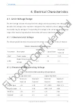
Page 23: ...absolute limit voltage ranges of FM101 NA 20 module Table 8 Absolute limit voltage range Parameter Description Minimum Value V Typical Value Maximum Value V VBAT Power supply 0 3 3 8 5 25 GPIO Digita...

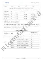
Page 24: ...r supply is described in the following table For AT commands used for USB sleep and wakeup see Fibocom_FM101_AT Commands User Manual Table 11 Power consumption Parameter Mode Status Average Current Ty...

Page 25: ...wakeup TBD Paging Cycle 128 USB wakeup TBD Paging Cycle 256 USB wakeup TBD TDD LTE Paging Cycle 32 USB wakeup TBD Paging Cycle 64 USB wakeup TBD Paging Cycle 128 USB wakeup TBD Paging Cycle 256 USB wa...

Page 26: ...BD Band26 23dBm TBD Band30 23dBm TBD Band66 23dBm TBD Band71 23dBm TBD TDD LTE Band41 23dBm TBD Band48 23dBm TBD Table 12 2CA power consumption 2CA Typical Combination Transmitting Band FRB Data Trans...

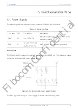
Page 27: ...is recommended GND G 3 5 11 27 33 39 45 51 57 71 73 GND all GND pins must be grounded Power Input The FM101 NA 20 module is powered on through the VBAT pin The following figure shows the recommended p...

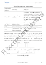
Page 28: ...Filter out low band RF interference 8 2pF 1800 1900 2100 2300 2500 2600 MHz band Filter out middle high band RF interference Stable power supply ensures proper operating of the FM101 NA 20 module Duri...

Page 29: ...8V DI 4 Module on off signal pull up to power on and pull down to power off In the power off state pull up the FCP for more than 1 2s The module is powered on 5 2 1 Power on off 5 2 1 1 Power on When...

Page 30: ...AT voltage is stable It is recommended that the time interval between powering on VBAT and pulling low or high the power on control pin is not less than 40ms The power on control is automatically pull...

Page 31: ...can be reset by hardware and software Table 16 Reset methods Reset Method Action Hardware reset Pull down the RESET_N pin for 0 5s or more and then release Software reset Send the AT CFUN 15 command F...

Page 32: ...ween two reset operations The RESET pin can be internally pulled up without external pull up Keep the pin floating when it is not used 5 3 LED1 The LED1 signal is used to indicate the operating status...

Page 33: ...module has built in U SIM card interface and supports 1 8 V and 3 0 V U SIM cards 5 4 1 U SIM Pin Definition U SIM pin definition is described in the following table Table 18 U SIM pin definition Pin...

Page 34: ...ection Active high by default And high level indicates a SIM card is inserted and low level indicates a SIM card is removed 1 8V 5 4 2 U SIM Interface Circuit U SIM Card Slot with Card Detection Signa...

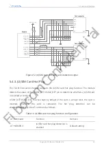
Page 35: ...ports the U SIM card hot plug function The module detects the status of the USIM1_DET USIM2_DET pin to determine whether a U SIM card is inserted or removed USIM1_DET USIM2_DET is active high by defau...

Page 36: ...M card slot shall not exceed 100 mm Longer cable will reduce signal quality The USIM_CLK and USIM_DATA signal lines are grounded and isolated to avoid mutual interference If conditions do not permit a...

Page 37: ...tion USB_DP AIO 7 USB 2 0 differential data signal USB_DM AIO 9 USB 2 0 differential data signal USB_SS_TX_M AO 29 USB 3 0 differential transmitting signal USB_SS_TX_P AO 31 USB 3 0 differential trans...

Page 38: ...with the maximum transmission rate of 480 Mbit s The following rules must be strictly followed in PCB layout USB_D and USB_D signal lines should have the differential impedance of 90 10 USB_D and USB...

Page 39: ...controlled as 90 7 Traces in the differential pair must be parallel with equal length and the length difference should be controlled less than 0 15 mm avoiding right angle traces Traces between diffe...

Page 40: ...TX Reserved I2S_MCLK DO 68 I 2 S main clock signal reserved Default transmission clock frequency is TBD MHz sampling rate is TBD KHz and resolution is TBD bit The PCM channel can also be configured as...

Page 41: ...3 PCIE_data transmitting signal positive PERn0 PCIE_RX_M 47 PCIE_Data receiving signal negative PERp0 PCIE_RX_P 49 PCIE_Data receiving signal positive PERST PCIE_RESET_N 50 PCIE mode reset signal CLKR...

Page 42: ...ifferent layers the via hole of ground signal should be close to that of signal and generally each pair of signals require 1 3 ground signal via holes and the traces shall never cross the segment of p...

Page 43: ...pecific requirements for the length match of transmitting pair and receiving pair that is the length match is only required in the internal differential lines rather than between different differentia...

Page 44: ...dule supports two ways as described in the following table to enter flight mode Table 24 Ways for module to enter flight mode 1 Hardware GPIO interface control Send AT GTFMODE 1 to turn on the hardwar...

Page 45: ...he module can be awakened by pulling down WAKEUP_IN pin Table 25 Sleep wakeup interface Pin Name I O Pin Number Description WAKEUP_IN DI 38 External device wake up module active low by default The mod...

Page 46: ...he RF main antenna for receiving and transmitting RF signals D refers to the diversity antenna for receiving diversity RF signals G refers to GNSS antenna 6 1 2 RF Connector Performance Rated Conditio...

Page 47: ...e is 818004607 from ECT company and the connector dimensions are 2 mm 2 mm 0 6 mm as shown in the following figure Figure 18 RF connector dimensions Figure 19 0 81 mm coaxial cable matched RF connecto...

Page 48: ...9 716 729 746 Band 13 LTE FDD 777 787 746 756 Band 14 LTE FDD 788 798 758 768 Band 17 LTE FDD 704 716 734 846 Band 25 LTE FDD 1850 1915 1930 1995 Band 26 LTE FDD 814 849 859 894 Band 30 LTE FDD 2305 2...

Page 49: ...50 dBm 23 5 dBm 2 dB LTE FDD 40 dBm 23 dBm 2 dB LTE TDD 40 dBm 23 dBm 2 dB 6 4 Receiving Sensitivity Table 28 FM101 NA 20 receiving sensitivity Mode Band Main Set Sensitivity Typ dBm Diversity Sensit...

Page 50: ...17 TBD TBD Band 25 TBD TBD Band 26 TBD TBD Band 30 TBD TBD Band 66 TBD TBD Band 71 TBD TBD LTE TDD Band 41 TBD TBD Band 48 TBD TBD 6 5 GNSS Receiving Performance The GNSS of FM101 NA 20 module suppor...

Page 51: ...obtained by testing some samples at 25 C 6 6 Antenna Design Antenna indicators The antenna requirements for FM101 NA 20 module are described in the following table Table 30 Module Antenna Requirement...

Page 52: ...rallel component grounded pins are connected directly to the main GND between the module and antenna connector or feeding point for antenna debugging This signal line impedance is controlled within 50...

Page 53: ...h If the line spacing is at least 3 times of the line width 70 of the electric field between the lines will not interfere with each other and this is called 3W principle Figure 21 3W principle 6 7 4 I...

Page 54: ...ating 25 PP 1080 65 Lay 4 0 33OZ Plating 25 Solder Mask The thickness from Lay 1 to Lay 2 is 65 um RF trace is 4 mil and the distance from RF to GND is greater than 3 times of RF line width The blue a...

Page 55: ...ntenna is placed outside the complete machine the antenna space is large and the antenna performance is not easy to be affected by the internal environment of the complete machine so that the antenna...

Page 56: ...ce RF ground shall be designed properly PCB board and edge of ground shall be provided with ground wall and antenna led from RF module shall be made into microstrip line The antenna RF feeding point p...

Page 57: ...It is recommended to design the antenna on the top of the device The distance between the signal point and GND point should be at least 4 mm to 5 mm The signal point and GND point can be put in differ...

Page 58: ...hich boasts a higher cost Attached Attach the metal sheet radiator to the back cover of the module Feed point of PIFA antenna The feeding point must be greater than 2mm 3mm Try to place it at the edge...

Page 59: ...module output It is recommended to design the antenna on the top of the device The following figure shows the monopole antenna design 9 0mm 5 0mm Antenna PCB motherboard Figure 28 Antenna location Ma...

Page 60: ...GSM DCS PCS 6 mm 35 mm x 8 mm GSM850 GSM900 DCS1800 PC S1900 6 mm 40 mm x 10 mm For details about CDMA EVDO WCDMA LTE TD SCDMA antenna design refer to the area requirement of GSM antenna IFA antenna I...

Page 61: ...sign of Internal Antenna 6 8 3 1 Handling of Speaker Connecting beads or inductors on speaker can reduce the impact on RF 6 8 3 2 Handling of Metal Structural Parts All the metal structural parts must...

Page 62: ...ht beside the antenna 6 8 3 4 Location of Large Components in Antenna Area Do not place large metal components such as oscillator speaker and receiver around the antenna they may greatly affect the el...

Page 63: ...e performance of module and the radiated power of antenna meet requirement then low sensitivity may be caused by main board design issue Poor coupling sensitivity is caused by poor circuit design of L...

Page 64: ...arallel to improve the receiving throughput The function of MIMO antenna is similar to that of diversity antenna and they both can resist against fading and improve throughput The customer is recommen...

Page 65: ...ces please refer to the recommended design If the application scenario and the recommended design are not consistent please contact FIBOCOM technicians for confirmation 6 Radio Frequency Copyright Fib...

Page 66: ...through the motherboard The following fogure shows the design Other measures to improve heat dissipation performance are as follows Heat devices and other heat sources on the motherboard are as far aw...

Page 67: ...ddition to ESD in packaging customers should consider the recommended circuit of the interface design in the document during module application The following table describes the ESD discharge range al...

Page 68: ...e is shown in the following figure Figure 32 Product appearance 9 2 Structural Dimensions The structural dimensions of the FM101 NA 20 module is shown in the following figure The unit is mm 9 Structur...

Page 69: ...torage transportation and usage The module is a precision electronic product and may suffer permanent damage if no correct electrostatic protection measures are taken Tray Package The FM101 NA 20 modu...

Page 70: ...mm 6 5 mm as shown in the following figure Figure 35 Tray size unit mm 9 4 Storage Storage conditions recommended The temperature is 23 5 and the relative humidity is less than RH 60 9 Structural Spec...

Page 71: ...Storage period Under the recommended storage conditions the storage life is 12 months 9 Structural Specifications Copyright Fibocom Wireless Inc 69 F i b o c o m C o n f i d e n t i a l...

Page 72: ...n Duplexing HSDPA High Speed Down Link Packet Access Imax Maximum Load Current LED Light Emitting Diode LTE Long Term Evolution ME Mobile Equipment MS Mobile Station MT Mobile Terminated PCB Printed C...

Page 73: ...unications System U SIM Universal Subscriber Identity Module Vmax Maximum Voltage Value Vnorm Normal Voltage Value Vmin Minimum Voltage Value VIHmax Maximum Input High Level Voltage Value VIHmin Minim...

Page 74: ...ue VOHmin Minimum Output High Level Voltage Value VOLmax Maximum Output Low Level Voltage Value VOLmin Minimum Output Low Level Voltage Value VSWR Voltage Standing Wave Ratio WCDMA Wideband Code Divis...

Page 75: ...ost manufacturer for Part 15 B requirements if needed Important Note notice that any deviation s from the defined parameters of the antenna trace as described by the instructions require that the host...

Page 76: ...s Reorient or relocate the receiving antenna Increase the separation between the equipment and receiver Connect the equipment into an outlet on a circuit different from that to which the receiver is c...

Page 77: ...na As long as 2 conditions above are met further transmitter test will not be required However the OEM integrator is still responsible for testing their end product for any additional compliance requi...

Page 78: ...uld be installed and operated with minimum distance 20 cm between the radiator your body D claration d exposition aux radiations Cet quipement est conforme aux limites d exposition aux rayonnements IS...

Page 79: ...cluding the transmitter and obtaining a separate Canada authorization NOTE IMPORTANTE Dans le cas o ces conditions ne peuvent tre satisfaites par exemple pour certaines configurations d ordinateur por...

Page 80: ...all required regulatory information warning as show in this manual Manuel d information l utilisateur final L int grateur OEM doit tre conscient de ne pas fournir des informations l utilisateur final...

Reviews: